SPRABJ8B September 2022 – November 2023 AM2631 , AM2631-Q1 , AM2632 , AM2632-Q1 , AM2634 , AM2634-Q1 , AM263P4
2.5.1.2 Digital/Analog I/O Power 3.3 V
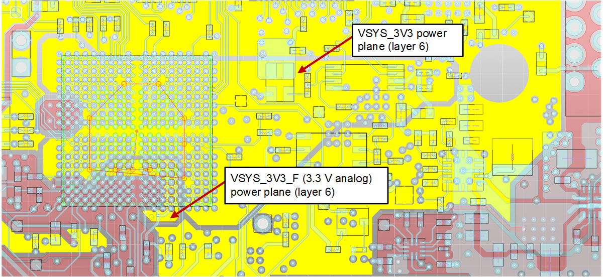
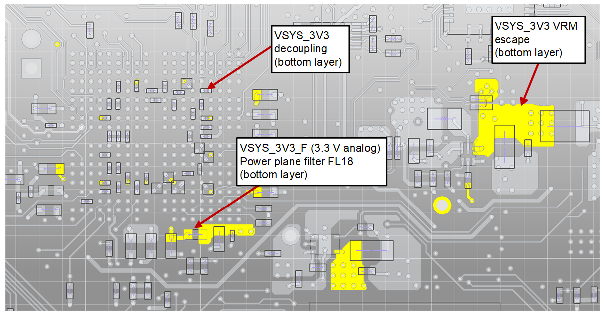
Z11 simulations were performed on the 3.3 V digital and analog power net of the controlCard EVM to verify transient power margin. The simulation domain included the:
- AM263x BGA (U1) 3.3V power and ground return BGA and fan-out
- Internal power and ground return routing layers
- Regulator output
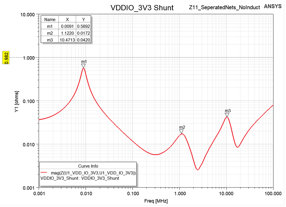
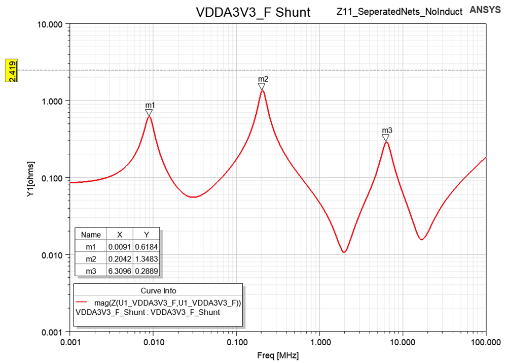
Initial runs of these simulations showed that no BOM changes were needed to meet the maximum and minimum frequency bandwidth below Ztarget (see above sections). Only the initial simulation with the final chosen BOM iterations are shown below.
The simulations were divided between the VDDS33 digital 3.3 V plane and decoupling network and the VDDA33 analog 3.3 V traces and decoupling local to the design. The F dividing line between these simulations is the FL18 ferrite bead element was used to separate these two decoupling performance simulations.
 Figure 2-14 AM263x LaunchPad PDN
Simulations – 3.3 V Digital/Analog I/O Power Simulation Domain (A)
 Figure 2-15 AM263x LaunchPad PDN
Simulations – 3.3 V Digital/Analog I/O Power Simulation Domain (layer 8,
bottom)
 Figure 2-16 AM263x LaunchPad PDN
Simulations – 3.3 V Digital I/O Power Simulated Z11
 Figure 2-17 AM263x LaunchPad PDN
Simulations – 3.3 V Analog I/O Power Simulated Z11