SPRACI7A October 2018 – March 2022 TMS320F280021 , TMS320F280021-Q1 , TMS320F280023 , TMS320F280023-Q1 , TMS320F280023C , TMS320F280025 , TMS320F280025-Q1 , TMS320F280025C , TMS320F280025C-Q1 , TMS320F280040-Q1 , TMS320F280040C-Q1 , TMS320F280041 , TMS320F280041-Q1 , TMS320F280041C , TMS320F280041C-Q1 , TMS320F280045 , TMS320F280048-Q1 , TMS320F280048C-Q1 , TMS320F280049 , TMS320F280049-Q1 , TMS320F280049C , TMS320F280049C-Q1 , TMS320F28P550SG , TMS320F28P550SJ , TMS320F28P559SG-Q1 , TMS320F28P559SJ-Q1
2.1 Memory Test Flow
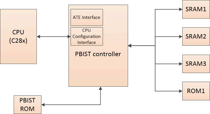
M-POST is enabled with the help of a Programmable Built in Self-Test (PBIST) solution, which is used for the manufacturing test of the device. PBIST has a CPU configurable interface used for field self-test in addition to the Automated Test Equipment (ATE) interface used during manufacturing test.
The PBIST architecture consists of a controller which is specifically designed toward efficient memory testing. The controller is designed with a dedicated register set and a highly specialized pipeline and instruction set targeted specifically toward testing memories. Furthermore, the PBIST engine is equipped with multiple read and multiple write memory ports, or buses, which enable it to efficiently test multiple memory instances in parallel. The PBIST controller also has access to the PBIST ROM. The PBIST ROM is where test routines are stored for the PBIST engine to fetch and execute. These test routines are fetched by the PBIST controller and executed on multiple on-chip memory instances in parallel. Because of the specialized architecture and test routines, PBIST provides very high diagnostic coverage on the implemented SRAMs and ROMs at a transistor level in a very efficient manner. Because PBIST controller has direct access to the ROMs and SRAMs, it is even able to test secure memory instances on devices equipped with DCSM (Dual Zone Code Security Module). For details on leveraging the DCSM on F28004x, see Achieving Coexistence of Safety Functions for EV/HEV Using C2000™ MCUs.
 Figure 2-1 PBIST Architecture
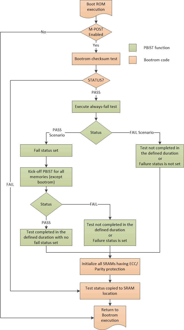
The steps involved in the execution of memory self-test are described in Figure 2-2.
 Figure 2-2 M-POST Execution Flow
- If enabled by configuring customer-OTP, M-POST is executed during every Power-ON reset sequence. Test is executed only during Power-ON reset and not during other resets (XRSn, WDRSn, Debugger reset, and so forth).
- Since the code for testing of the memories resides in boot rom, it is not be possible to test the boot rom using PBIST. Hence a separate boot-rom checksum test will be done prior to PBIST. If the boot-rom checksum test fails, rest of PBIST test is not executed. The test status is copied to SRAM.
- Prior to performing any test using PBIST, an always fail test case is executed. This is to validate the proper functioning of the PBIST controller and its ability to indicate failure. The test status bits are registered on completion of the test. If the test fails (i.e. always fail test passes), the entire test sequence is bypassed and test status is returned to the application code. If the test passes, the complete set of device memories (except boot-rom) is tested in the next phase.
- All the SRAMs are tested using March13n and all the ROMs other than boot-rom will be tested using ROM signature computation algorithm.
- Once the test is complete, all the CPU RAMs are initialized.
- Timeout feature is implemented during each of the test sequence to identify whether the test is completing during the stipulated time or getting delayed due to a fault.
- The status of the PBIST test (test not executed due to failure of checksum test, always fail test status, memory self-test status and timeout error) are communicated to the application.
- The device will not be fit to run any functional safety application if the memory test is failing. Boot-rom will let the application code determine the future course. The application may fire NMI (using software) and let the external devices know about the failure using ERROR_STS pin.
- If the start-up memory test is failing, application will not have enough information to identify the failing memory. Application may have to run diagnostics for this. The diagnostics sequence may be to execute tests on individual memory instances and identify the failing memory.