SPRACP7 October 2019 AM6526 , AM6528 , AM6546 , AM6548
3.2 Multi-Domain Time Synchronization Across PCIe Interconnect
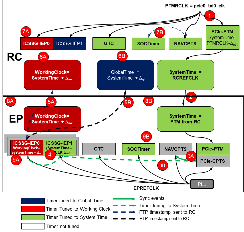
In the second example, the scenario where two AM65xx devices are deployed is considered: one as host processor and one as an interface processor, as shown in Figure 9. The interface device is connected to the host via PCIe.
 Figure 9. Time-Sync Use Case Example 2: Time Sychronization Across Two Devices
 In this example, the following time-bases should be maintained:
- System Time: this is the commonly understood time base between the two devices, when timestamp values are exchanged across them. Typically, all timestamps shall be based on the System Time. System Time can be synchronized via the PTM protocol across the PCIe link, where the RC designate its PHY clock as the System Time. In this example, the interface device acts as PTM Requester, it then tune the IEP1 timer in the ICSSG so its firmware can timestamp PTP packets based on the common System Time;
- Working Clock: this is sometimes referred as the communication time, it is the common time-base for network packet scheduling and traffic management. In this example, the device receives 802.1AS PTP streams from its network interface, then ICSSG firmware parses PTP streams and send out recorded timestamps to the host for 802.1AS protocol execution.
- Global Time: this is the time all time sensitive tasks obey in the domain. Typically these time-sensitive applications are scheduled based onthe Global Time. In this example, similar to the Working Clock, the Global Time is received on the Ethernet port via the IEEE 802.1AS protocol. The ICSSG firmware parses PTP packets and send timestamps to host where the actual protocol stack runs.
Some detailed configuration and software steps are:
- RC designate PTMRCLK = pcie0_txi0_clk as System Time and configure other timer modules to use this clock as timer tick
- RC sends system time to EP via PTM protocol
- EP receives updated PTM time, sync events are generated from PCIE to trigger time-stamping by both NAVSS-CPTS and ICSSG-IEP1. Rate and phase offset between EP-REFCLK and PTM: ∆ptm is recorded
- ICSSG-IEP1 is tuned by applying ∆ptm, then the tuned IEP1 is used to timestamp PTPs for Working Clock (WC) and Global Time (GT), and record:
- Twc: WC PTP stamped by System Time, there may be multiple timestamps according to 802.1AS
- Tgt: GT PTP stamped by System Time, there may be multiple timestamps according to 802.1AS
- Twc and Tgt are sent to RC by EP via PCIe interface (not part of PTM protocol);
- RC execute 802.1AS protocols to calculate working clock and global time, and also calculate:
- ∆wc :clock offset between Working Clock and System Time
- ∆gt: clock offset between Global Time and System Time
- RC tunes ICSSG-IEP0 for working clocking and tunes one of SoC Timers for Global Time
- RC sends ∆wc and ∆gt to EP via PCIe interface (software).
- At EP side, ICSSG0-IEP0 and one of the SOC timers are tuned to the WC and GT, respectively