SPRUJ09D March 2022 – September 2023 AM2631 , AM2631-Q1 , AM2632 , AM2632-Q1 , AM2634 , AM2634-Q1 , AM263P2-Q1 , AM263P4 , AM263P4-Q1
- 1
- Abstract
- Trademarks
- 1Preface: Read This First
- 2Control Card Overview
- 3Board Setup
- 4Hardware Description
- 5References
- Revision History
- A E2 Design Changes
- B E1 HSEC Pinout Table
4.4 Clock
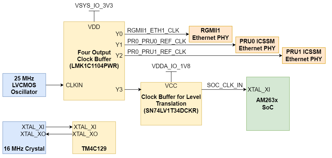
The AM263x SoC requires a 25-MHz clock input for XTAL_XI. All reference clocks required for the SoC and the three Ethernet PHY's are generated from a single four output clock buffer (LMK1C1104PWR), which is sourced from a single 25-MHz LVCMOS Oscillator by default. A clock buffer is used for level translation from 3.3 V to 1.8 V.
The Control Card also requires a 16-MHz clock source for the TM4C129 microcontroller for UART-USB JTAG support.
 Figure 4-5 Oscillator Clock Tree
Alternatively, the SoC clock input can be sourced from a single 25-MHz crystal. To use the crystal there must be resistors mounted and unmounted. When the Crystal is used as a clock source then the AM263x CLKOUT0 signal is used to source the four output clock buffer for the Ethernet PHY reference clock signals.
 Figure 4-6 Crystal Clock Tree
The following table describes the proper resistors to be mounted and DNI'd in order for each clock source configuration.
| Clock Source | Mounted | DNI |
|---|---|---|
| 25-MHz LVCMOS Oscillator (default) | R161, R135 | R158, R155, R134 |
| 25-MHz Crystal | R158, R155, R134 | R161, R135 |