SPRUJ09D March 2022 – September 2023 AM2631 , AM2631-Q1 , AM2632 , AM2632-Q1 , AM2634 , AM2634-Q1 , AM263P2-Q1 , AM263P4 , AM263P4-Q1
- 1
- Abstract
- Trademarks
- 1Preface: Read This First
- 2Control Card Overview
- 3Board Setup
- 4Hardware Description
- 5References
- Revision History
- A E2 Design Changes
- B E1 HSEC Pinout Table
4.17 ADC and DAC
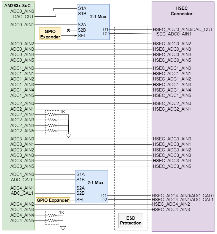
The AM263x Control Card supports 24 ADC signal channels that are mapped for the AM263x SoC and terminated to the HSEC connector. All ADC signals are ESD protected (TPD4E001DBVR).
 Figure 4-26 ADC HSEC Connections
There are two muxes (TMUX1136DQAR) that determine the pathing of ADC signals to and from the HSEC Connector.
Table 4-18 ADC MUX Select Logic
| MUX Select Signal | Condition | Function | Description |
|---|---|---|---|
| ADC1_MUX_SEL | SEL Signal HIGH | S1A → D1 | HSEC_ADC0_AIN0 selected |
| S2A → D2 | HSEC_ADC0_AIN1 selected | ||
| SEL Signal LOW | S1B → D1 | HSEC_DAC_OUT selected | |
| S2B → D2 | HSEC_DAC_OUT selected | ||
| ADC2_MUX_SEL | SEL Signal HIGH | S1A → D1 | HSEC_ADC4_AIN0 selected |
| S2A → D2 | HSEC_ADC4_AIN1 selected | ||
| SEL Signal LOW | S1B → D1 | ADC_CAL0 selected | |
| S2B → D2 | ADC_CAL1 selected |
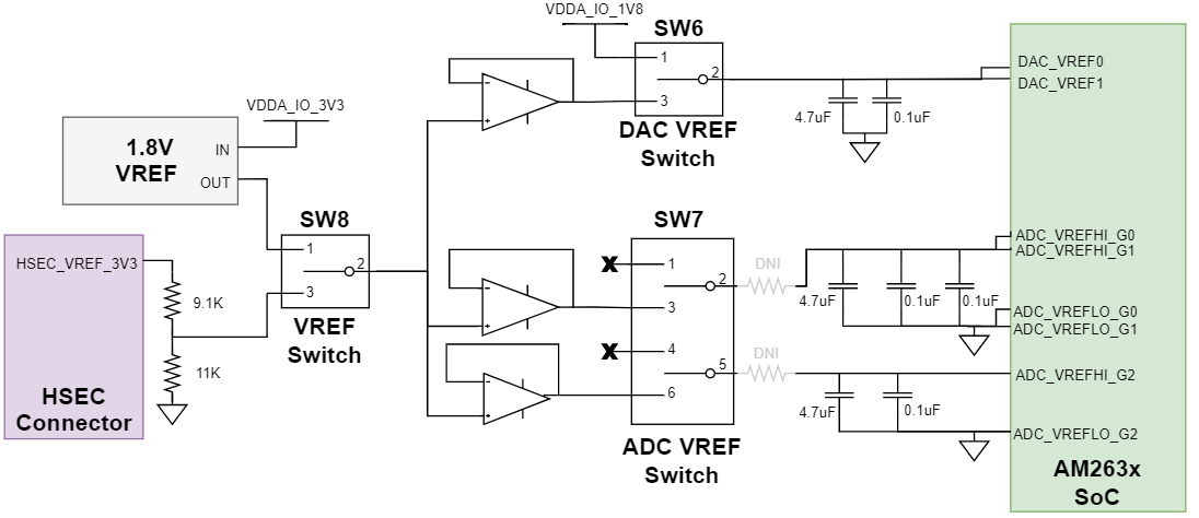
There are three switches that are used to configure the reference voltages for the ADC and DAC.
 Figure 4-27 ADC Switch Routing
- The VREF Switch (SW8) is a single
pole double throw switch that controls which 1.8 V reference will be used for
ADC and DAC.Table 4-19 VREF Switch
VREF Switch Position Reference Selection Pin 1-2 On board 1.8 V Reference (REF3318AIDBZT) Pin 2-3 HSEC VREF - The DAC VREF Switch (SW6) is a
single pole double throw switch that controls the input for the DAC VREF inputs
of the AM263x SoC.Table 4-20 DAC VREF Switch
DAC VREF Switch Position Reference Selection Pin 1-2 AM263x on-die LDO Pin 2-3 Output of VREF Switch - The ADC
VREF Switch (SW7) contains two single pole double throw switches that control
the input for the ADC VREF inputs of the AM263x SoC.Table 4-21 ADC VREF Switch
ADC VREF Switch Position Reference Selection Pin 1-2 OPEN - Allow for reference to be AM263x on-die LDO reference Pin 2-3 Output of VREF Switch Pin 4-5 OPEN - Allow for reference to be AM263x on-die LDO reference Pin 5-6 Output of VREF Switch