SSZTBA7 may 2016 66AK2L06 , ADC12J4000 , ADC32RF45 , ADS62P45 , LMK04828 , LMX2592
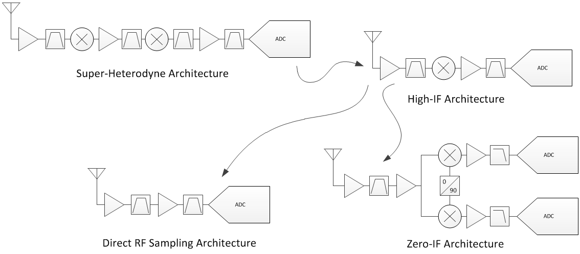
Radio receiver architectures, such as wireless communications and military systems have evolved drastically over the last decade, largely driven by innovation in high speed analog-to-digital converters (ADCs). Ten years ago, most radios were built using the basic super-heterodyne architecture with multiple downconversion stages. Around that time, we saw the move to a single downconversion stage in the high IF (intermediate frequency) architecture. This was driven by significant improvements in ADC bandwidth, sampling rates and performance that enabled sampling of signals in the second or third Nyquist zone. The ADS62P45 ADC is an example of a device that led this change. Now, further extraordinary advancements in ADC technology allows removal of the last downconversion stage in the radio in favor of the direct radio frequency (RF) sampling receiver; see Figure 1.
ADCs capable of being used in direct RF sampling radio architectures have been on the market for a few years, for example, TI’s ADC12J4000, however, the ADC32RF45 is the first ADC to enable direct RF sampling that rivals the dynamic range of super-heterodyne and high-IF architectures. In zero-IF architectures – the preferred architecture for extreme wideband systems – the ADC32RF45 is the first ADC to enable 2GHz of complex signal bandwidth with a single device.
 Figure 1 Radio Receiver Architecture
Evolution
Figure 1 Radio Receiver Architecture
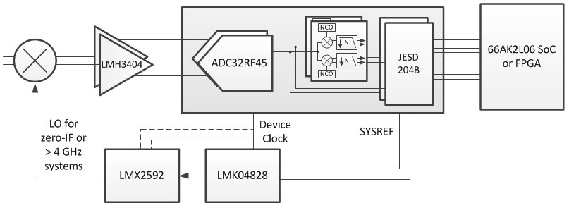
EvolutionAs most designers know, data-converter performance is only as good as other integrated circuits (ICs) in the system. The right devices can make (or break) your direct RF sampling receiver or wideband zero-IF receiver. Figure 2 shows some of the devices that make up the signal chain, take a look, because we are going to dig a little deeper into several of these devices.
 Figure 2 Direct RF Sampling
Signal-chain Solution
Figure 2 Direct RF Sampling
Signal-chain SolutionFive Components for Your RF Sampling Receiver or Wideband Digitizer
Selecting devices that complement each other can be challenging when simply looking at data sheets. In this post, I’ll give some background on five of the components in Figure 2, ADC included, that will complete, simplify and/or improve RF sampling or wideband zero-IF receivers. This solution could be used in wireless infrastructure, military radar, electronic warfare, or wideband communications test equipment systems.
Data Conversion
The ADC32RF45 is the heart and soul of this RF sampling receiver. It has a noise floor of -155dBFS/Hz, enabling direct sampling of signals at RF frequencies up to 4GHz; however, it needs a high-quality sampling clock to avoid degrading the dynamic range achieved by high-IF architectures. For signals above 4GHz, you can use the ADC32RF45 in a wideband high-IF or zero-IF architecture with the help of an RF synthesizer. The high sampling rate, combined with two channels in a single package, means you can use the smallest 2GHz signal bandwidth zero-IF receiver and minimize I/Q mismatch between ADC channels – but only with a driving amplifier that is also small and well matched.
The ADC32RF45 includes four integrated digital downconverters (DDCs), two per channel, to offload logic device processing. The DDCs can mix the desired signal down to I/Q baseband using up to three numerically controlled oscillators per channel for observation or carrier-hopping applications. A decimation filter then lowers the data rate to enable direct RF sampling, giving you the benefits of high ADC sample rates while reducing signal-processing and ADC interface requirements. The decimated signal is then sent to a field-programmable gate array (FPGA) or digital signal processor (DSP) for additional baseband processing.
Amplification and Single-ended to Differential Conversion
An amplifier drives ADCs in both direct RF sampling and wideband zero-IF architectures. The LMH3404 dual-channel, fully differential amplifier works well with the RF sampling ADC in systems operating from DC to 2GHz, thanks to the LMH3404’s 7GHz bandwidth. The LMH3404 is designed to be a transformer (balun) replacement for performing single-ended to differential signaling conversion for an ADC while providing 18dB of gain. It also has an advantage over transformers, operating all the way down to DC, which wideband zero-IF systems require. Paired with the ADC32RF45, the LMH3404 creates a small and higher-performance 2GHz-bandwidth zero-IF receiver for wideband communications and testing. The dual-channel amplifier has excellent gain and phase matching between channels, limiting the amount of digital mismatch correction these systems require.
Clocking
In an RF sampling radio, the quality of the sampling clock has a strong effect on the system’s resulting signal-to-noise ratio (SNR). The LMK04828, a JESD204B-compliant ultra-low noise clock jitter cleaner, can generate RF sampling-capable clocks with <100fs of jitter while offering an array of features to shrink or simplify the system. With support for up to seven JESD204B devices, the LMK04828 can clock multiple ADC32RF45 ADCs, digital-to-analog converters (DACs), FPGAs or DSPs. The LMK04828 can also generate the SYSREF signal, used for deterministic latency in JESD204B systems, while digital and analog delays help you meet critical timing requirements for each JESD204B device.
For systems with extremely high-quality clocks, the LMK04828 can act as a clock-distribution device while still allowing SYSREF generation and delay capabilities. I recommend the LMK04828 for all ADC32RF45-based systems.
RF Synthesis
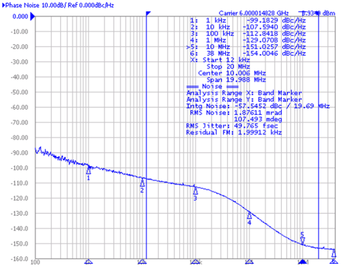
Another option for high-performance clocking – critical for direct RF sampling architectures – is to use the LMX2592 RF synthesizer in conjunction with the LMK04828. The LMX2592’s high output swing and low phase noise allow it to achieve <50fs root mean square (RMS) jitter with a 12kHz-20MHz integration bandwidth, as shown in Figure 3, enabling multidecibel improvements in SNR at high RFs frequencies. The LMK04828 acts as a reference clock for the LMX2592 while also generating SYSREF signals for JESD204B subclass-1 deterministic latency.
 Figure 3 LMX2592 Jitter Performance at 6GHz Output Frequency
For systems with carrier frequencies above 4GHz (C-band or X-band), the LMX2592 can act as a local oscillator (LO), generating signals of up to 9.8GHz, to mix the desired signal down to a relatively high IF of up to 4GHz. The ADC32RF45 can directly sample IF signals with bandwidths as high as 1GHz, creating a wideband, high-frequency, high-IF architecture.
Alternatively, the LMX2592 can act as an LO in a zero-IF architecture, enabling as much as 2GHz of signal bandwidth when paired with the ADC32RF45.
Digital Signal Processing
The ADC32RF45 typically interfaces with FPGAs; however, the JESD204B digital output of the ADC32RF45 can connect directly to the 66AK2L06 multicore digital signal processor (DSP) plus ARM® system-on-chip (SoC) when using some of the ADC’s DDC functionality. Direct connection of the ADC32RF45 to the SoC reduces size, weight and power (SWaP) from the system by removing an interconnect FPGA.
The 66AK2L06 contains a programmable digital front-end (DFE) with DDC and digital-filtering capabilities that extend the ADC32RF45’s processing functionality, allowing additional sub-banding or filtering for multicarrier RF systems. Additionally, the DFE contains automatic gain control (AGC) functionality to protect the ADC32RF45 while maintaining optimal ADC performance. The “DFE User Guide for Keystone II Devices” provides more insight into ADC32RF45 functionality, and the allowable number of JESD204B lanes and rates. The 66AK2L06 SoC integrates fast fourier transform coprocessors (FFTC) to accelerate the complex FFT/iFFT operations by 10-15x, ideal for low-latency applications.
Conclusion
The ADC32RF45 enables designers to architect direct RF sampling radios without having to make dynamic-range trade-offs. The best-in-class signal-chain components from TI mentioned in this post maximize system performance with the ADC32RF45:
- The LMH3404 can act as a DC to 2GHz ADC driver and as a transformer (balun) replacement for single-ended to differential conversion capable of DC coupling and providing 18dB of gain.
- The LMK04828 generates or distributes high-performance clocks required for RF sampling.
- The LMX2592 offers an even higher-performance clocking option, acting as an LO synthesizer for systems whose carrier frequencies exceed 4GHz (C-band or X-band).
- Connecting the JESD204B output to the 66AK2L06 DSP can reduce SWaP.
If you will be at IMS2016 from May 22 – 27 in San Francisco, you will be able to test the ADC32RF45 yourself. The ADC32RF45 will be featured at booth 419. Please stop by! For everyone else, subscribe to the Analog Wire blog to be the first to know when we post the next RF sampling blog post.
Additional Resources
- Read this 10-part RF sampling blog series.
- Watch RF sampling videos on the High Speed Signal Chain University website.
- Read the white paper, “Direct RF conversion: From vision to reality.”
- Read more about implementing JESD204B SYSREF in the application note, " Implementing JESD204B SYSREF and Achieving Deterministic Latency With ADC32RF45."