SWRA730 February 2022 CC1311P3 , CC1311R3 , CC1312R , CC1312R7 , CC1314R10 , CC1352P , CC1352P7 , CC1352R , CC1354P10 , CC1354R10
- Trademarks
- Acronyms
- 1Description of the PCB Antenna
- 2Test Setup
- 3Unmatched Results
- 4Single-Band Matching and Result
-
5Dual Band Matching and Results
- 5.1 433-MHz and 2440-MHz Smith Chart, SWR, Bandwidth, and Efficiency
- 5.2 470-MHz and 2440-MHz Smith Chart, SWR, Bandwidth and Efficiency
- 5.3 490 MHz and 2440 MHz Smith Chart, SWR, Bandwidth and Efficiency
- 5.4 510-MHz and 2440-MHz Smith Chart, SWR, Bandwidth, and Efficiency
- 5.5 868/915 and 2440-MHz Smith Chart, SWR, Bandwidth, and Efficiency
- 6Summary - Bill of Materials and Results
- 7Conclusion
- 8References
1.1 Implementation of the PCB Meander Monopole Antenna
To obtain optimum performance, it is important to make an exact copy of the antenna dimensions. The antenna was implemented on a 1.6-mm thick FR4 substrate. Since there is no ground plane beneath the antenna, the PCB thickness is not critical. If a different thickness is used then it could be necessary to change the matching network to obtain optimum performance.
One approach to implement the antenna in a PCB CAD tool is to import the antenna layout from a Gerber file. Refer to files included in the LAUNCHXL-CC1352P-4 Reference Design.
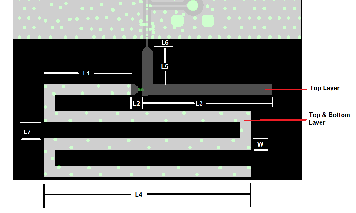
If the antenna is implemented on a PCB that is wider than the antenna it is important to avoid placing components or having a ground plane close to each side of the antenna. If the CAD tool being used does not support import of Gerber files, Figure 1-1 and Table 1-1 can be used.
 Figure 1-1 LAUNCHXL-CC1352P-4
| L1 | 16.0 mm | L5 | 7.0 mm |
| L2 | 2.0 mm | L6 | 1.4 mm |
| L3 | 24.0 mm | L7 | 3.0 mm |
| L4 | 38.0 mm | W | 2.0 mm |
The last antenna segment's optimum length will always be dependent on the geometry of the ground plane. For ground plane sizes smaller than the LAUNCHXL-CC1352P-4 (less than a quarterwave), the optimum length of the last segment could be increased or the antenna match re-calculated for the new ground plane size.