TIDT244 July 2021
4.4 Current Loop to Voltage Loop Transition
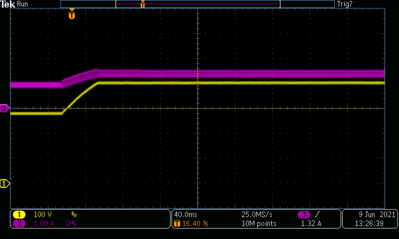
The following figure shows the transition between the current loop control mode and the voltage loop control mode.
In the beginning state, the board is set to 1 A of output current and 400 V of output voltage. The resistive load is set to 270 Ω. In this state, the load is attempting to draw more current than the 1 A current limit allows. This means that the output voltage is limited to 270 V and the current loop is in control.
In the end state, the board output current setting is changed from 1 A to 2 A. The increased current limit is more than the current draw of the load. This allows the output voltage to rise up to the commanded 400 V and the voltage control loop takes over.
 Figure 4-10 VIN = 400 V, VOUT = 400 V. Resistive Load = 270 Ω (VOUT: 100 V/DIV, IOUT: 1 A/DIV, 40 ms/DIV, BWL = 20 MHz)