TIDUEH2C April 2021 – September 2022
2 System Overview
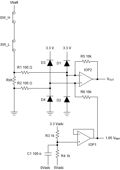
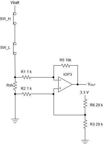
One concern of low-side current sense circuits is that large and/or very fast currents will cause the local ground voltage to change beneath the shunt due to ground plane impedance. Therefore, a difference-amplifier configuration (Figure 2-1 and Figure 2-2) is needed to measure the differential voltage directly across the shunt resistor.
Non-inverting gain and inverting gain give similar results, and either gain polarity can be used to satisfy hardware system requirements.
To measure a bidirectional current with a single positive supply, the output voltage for 0-A must be offset to mid-supply, by providing a reference voltage (Figure 2-1, VREF) to the amplifier. A convenient way to ensure this reference voltage is quiet and referenced to the same analog ground as the ADC, is to place a voltage divider close to the microcontroller's analog voltage reference inputs, and to use another amplifier (Figure 2-1, IOP1) to buffer this voltage. The reference amplifier can supply this low noise, low impedance, mid-supply reference voltage to all three low-side shunt monitor amplifiers.
 Figure 2-1 Difference Amplifier with Analog Ground Reference Voltage and Input Protection Diodes
 Figure 2-2 Difference Amplifier with Local Thévinin Equivalent Reference Voltage
In low cost, lower-current applications, the voltage-reference amplifier and 10kΩ series resistor (Figure 2-1, R6) can be replaced with a Thévenin-equivalent resistor divider, for each amplifier, as has been done in this reference design. The drawback of using an unbuffered voltage divider is that when the amplifier is next to the shunt, the ground bounce caused by the large shunt current might be included in the reference voltage, and thereby offset the measurement sent to the ADC.