TIDUEO1B April   2021  – June 2021


  1.   Description
  2.   Resources
  3.   Features
  4.   Applications
  5.   5
  6. 1General Texas Instruments High Voltage Evaluation (TI HV EVM) User Safety Guidelines
  7. 2System Description
    1. 2.1 Key System Specifications
  8. 3System Overview
    1. 3.1 Block Diagram
    2. 3.2 Design Considerations
      1. 3.2.1 Basic Operation
      2. 3.2.2 PCMC PSFB using C2000
    3. 3.3 System Design Theory
      1. 3.3.1 Peak Current Mode Control (PCMC) Implementation
      2. 3.3.2 Zero Voltage Switching (ZVS) or Low Voltage Switching (LVS)
      3. 3.3.3 Synchronous Rectification
      4. 3.3.4 Slope Compensation
    4. 3.4 Highlighted Products
      1. 3.4.1 C2000™ MCU F28004x
  9. 4Hardware, Software, Testing Requirements, and Test Results
    1. 4.1 Required Hardware and Software
      1. 4.1.1 Hardware
      2. 4.1.2 Software
        1. 4.1.2.1 Software Control Flow
        2. 4.1.2.2 Incremental Builds
        3. 4.1.2.3 Procedure for running the incremental builds - PCMC
          1. 4.1.2.3.1 Build 1: Peak Current Loop Check with Open Voltage Loop
            1. 4.1.2.3.1.1 Objective
            2. 4.1.2.3.1.2 Overview
            3. 4.1.2.3.1.3 Procedure
              1. 4.1.2.3.1.3.1 Start CCS and Open a Project
              2. 4.1.2.3.1.3.2 Build and Load the Project
              3. 4.1.2.3.1.3.3 Debug Environment Windows
              4. 4.1.2.3.1.3.4 Using Real-Time Emulation
              5. 4.1.2.3.1.3.5 Run the Code
          2. 4.1.2.3.2 Build 2: Closed current and voltage loop (Full PSFB)
            1. 4.1.2.3.2.1 Objective
            2. 4.1.2.3.2.2 Overview
            3. 4.1.2.3.2.3 Procedure
              1. 4.1.2.3.2.3.1 Build and Load Project
              2. 4.1.2.3.2.3.2 Debug Environment Windows
              3. 4.1.2.3.2.3.3 Run the Code
      3. 4.1.3 Test results
  10. 5Design and Documentation Support
    1. 5.1 Design Files
      1. 5.1.1 Schematics
      2. 5.1.2 BOM
    2. 5.2 Software
    3. 5.3 Documentation Support
  11. 6Terminology
  12. 7About the Author
  13. 8Revision History

Basic Operation

A PSFB converter consists of four-power electronic switches (like MOSFETs or IGBTs) that form a full-bridge on the primary side of the isolation transformer and diode rectifiers or MOSFET switches for synchronous rectification (SR) on the secondary side. This topology allows the switching devices to switch with zero voltage switching (ZVS) resulting in lower switching losses and an efficient converter.

For such an isolated topology, signal rectification is required on the secondary side. For systems with low output voltage and/or high output current ratings, implementing synchronous rectification instead of diode rectification achieves the best possible performance by avoiding diode rectification losses. In this work, synchronous rectification is implemented on the secondary side.
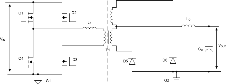
GUID-20201007-CA0I-M0MH-XMCS-FQZL59529MPS-low.gif Figure 3-2 A Phase-Shifted Full Bridge Circuit
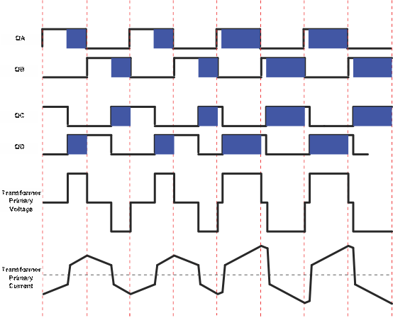
Figure 3-2 shows a simplified circuit of a phase shifted full-bridge. MOSFET switches Q1, Q4, Q2 and Q3 form the full-bridge on the primary side of the transformer T1. Q1 and Q4 are switched at 50 % duty and 180 degree out of phase with each other. Similarly, Q2 and Q3 are switched at 50 % duty and 180 degree out of phase with each other. The PWM switching signals for leg Q2 – Q3 of the full-bridge are phase shifted with respect to those for leg Q1 - Q4. Amount of this phase shift decides the amount of overlap between diagonal switches, which in turn decides the amount of energy transferred. D5, D6 provide diode rectification on the secondary(MOSFETs used in our design for SR), while Lo and Co form the output filter. Shim inductor LR provides assistance to the transformer leakage inductance for resonance operation with MOSFET capacitance and facilitates Zero Voltage Switching (ZVS). The switching waveforms for the system are shown in Figure 3-3.
GUID-3245FE21-DFED-4AC8-96F1-04197921C33A-low.gif Figure 3-3 PSFB PWM Waveforms