TIDUEO1B April 2021 – June 2021
- Description
- Resources
- Features
- Applications
- 5
- 1General Texas Instruments High Voltage Evaluation (TI HV EVM) User Safety Guidelines
- 2System Description
- 3System Overview
-
4Hardware, Software, Testing Requirements, and Test Results
- 4.1 Required Hardware and Software
- 5Design and Documentation Support
- 6Terminology
- 7About the Author
- 8Revision History
4.1.1 Hardware
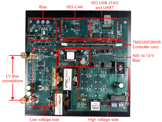
Figure 4-1 shows key hardware components. This hardware uses the kit of Bidirectional 400-V/12-V DC/DC Converter Reference Design as the base board and with some modification for peak current mode control.
 Figure 4-1 TIDM-02000 hardware
The key signal connections between the controlCARD and the base board are listed in the Table 4-1
|
SIGNAL NAME |
DESCRIPTOIN |
CONNECTION TO CONTROLCARD |
|---|---|---|
| ePWM-1A | PWM drive for full-bridge switch Q2 | GPIO-00 |
| ePWM-1B | PWM drive for full-bridge switch Q3 | GPIO-01 |
| ePWM-2A | PWM drive for full-bridge switch Q1 | GPIO-02 |
| ePWM-2B | PWM drive for full-bridge switch Q4 | GPIO-03 |
| ePWM-4A | PWM drive for sync rectifier/push-pull switch Q6 | GPIO-07 |
| ePWM-4B | PWM drive for sync-rectifier/push-pull switch Q5 | GPIO-06 |
| VLV-FB | Low voltage bus – voltage feedback | ADC-A0 |
| ILV-FB | Low voltage current feedback (Jumper J2 populated) | ADC-B3/COMP2A |
| ILV-FILT | Heavily filtered low voltage current feedback | ADC-B2 |
| VHV-FB | High voltage bus – voltage feedback | ADC-B1 |
| IHV-FB | Transformer high voltage winding current | ADC-A2/COMP1A |
| IHV-FILT | Heavily filtered transformer high voltage winding current | ADC-A1 |
This board provides a lot of jumper options for experimentation but there are some jumpers that must be populated for proper operation of the board. These jumpers that must be populated are listed below:
C:JPG1, E:JPG1, J2, J5, J6, J7, J8, J10, J11, J12, J13, J15, J16, and J19.
Some hardware modifications are required by the customer before running the reference code in this board.
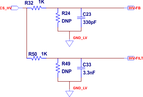
 Figure 4-2 Peak Current Sensing Circuit
- Remove resistor R50 in Figure 4-2. The heavily filtered winding current of the CT on the secondary side is used for average current mode control. For peak current mode control, a relatively low cutoff frequency filter is needed. Existence of R50 can introduce distortion to the current waveform.
Notes: Some magnetic components in the original board are replaced for peak current mode control as shown in Table 4-2.
CURRENT | ORIGINAL | |
|---|---|---|
| Main transformer | MPS P6524_A | VITEC AF5551R |
| Secondary side inductor | VITEC 6193R | VITEC AF5666BR |
| Shim inductor | VITEC 6194R | VITEC AF5667BR |
ControlCARD settings:
Certain settings on the device control card are required to communicate over JTAG and use the isolated UART port. The user must also provide a correct ADC reference voltage. The following settings are required for revision A of the TMS320F280049C control card (refer to the info sheet located at \c2000ware\boards\controlCARDs\TMDSCNCD280049C.
- Set both ends of S1:A on the control card to ON (up) position to enable JTAG connection to the device and UART connection for SFRA GUI. If this switch is OFF (down), the user cannot use the isolated JTAG built in on the control card, nor can the SFRA GUI communicate with the device.
- Connect the USB cable to J1:A to communicate with the device from a host PC on which CCS runs.
- For the control loop, use the internal reference of the TMS320F28004x and move the S8 switch to the left (that is, pointing to VREFHI).
- For best performance of this reference design, remove the capacitor connected between the isolated grounds on the control card, C26:A.