TIDUF28 November 2023
- 1
- Description
- Resources
- Features
- Applications
- 6
- 1System Description
- 2System Overview
- 3System Design Theory
-
4Hardware, Software, Testing Requirements,
and Test Results
- 4.1 Hardware Requirements
- 4.2 Software Requirements
- 4.3 Test Setup
- 4.4 Test Results
- 5Design and Documentation Support
- 6About the Author
4.4.3 Switch Node Transient at 320-VDC Bus Voltage
The C2000 MCU was configured to generate a 3-phase space vector with complementary PWM with 16-kHz switching frequency and 150-ns dead time. The PWM duty cycle per phase was configured to drive the corresponding phase DC current IU with IV = IW = –0.5 IU.
The LMG3422 switch node voltage at phase U was measured with a pigtail probe at the top of the LMG3422 source versus PGND inserted into the two vias, prepared for testing, as shown in Figure 4-6.
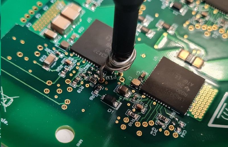 Figure 4-6 LMG3422 Switch Node Phase Voltage Measurement
The following figures outline the phase U switch node transient at phase currents ±1 A and ±4 A to illustrate hard-switching and soft-switching.
Observe that at ±1 A, the phase current U is not large enough to discharge (or charge) the effective output capacitance of the half-bridge during the short dead time of 120 ns; therefore, the corresponding GaN-FETs are still partially hard-switching, but at a lower drain-to-source voltage. For example with Figure 4-7, the top GaN-FET turns off and the bottom GaN-FET turns into the 3rd quadrant mode. Due to the parasitic output capacitance, the phase U voltage decline is impacted by the effective parasitic output capacitance of each half-bridge. After the 120-ns dead time, the effective parasitic output capacitance is discharged with the impressed current of 1 A from 320 V to around 250 V. Hence the bottom-side GaN-FET is still hard switched from 250 V to 0 V.
The phase current oscillations (4.5 Apeak, around 10 MHz, 500-ns duration in hard-switching) seen with Figure 4-7 through Figure 4-14 are due to the parasitic capacitance and inductance of the 1-m cable and the AC induction motor.
The oscillations significantly reduce when using a 20-cm cable, in that case with a 200 VAC servo motor, as shown in Figure 4-15 and Figure 4-16.
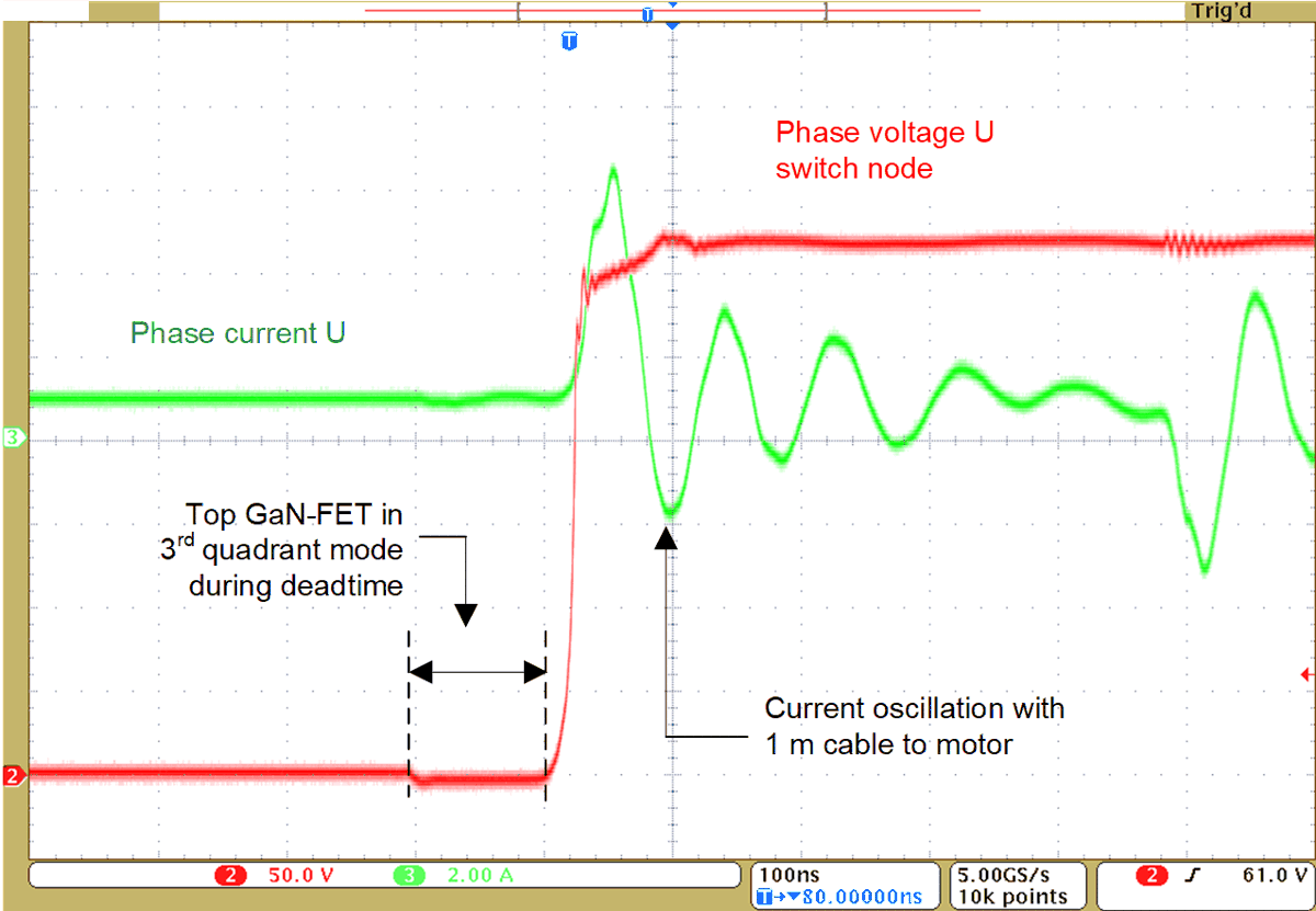 Figure 4-7 Phase U Rising Edge Waveform at 1 A, 1-m Cable to AC Induction Motor
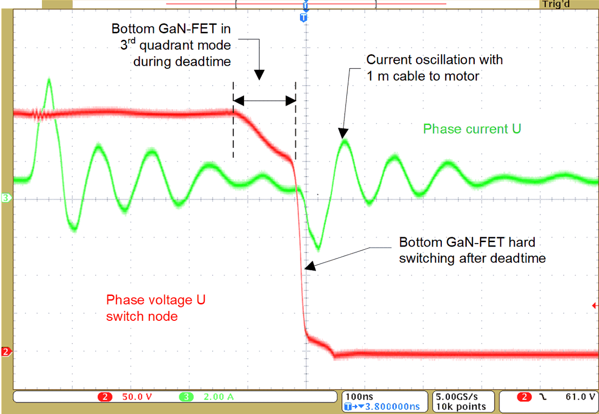 Figure 4-8 Phase U Falling Edge Waveform at 1 A, 1-m Cable to AC Induction Motor
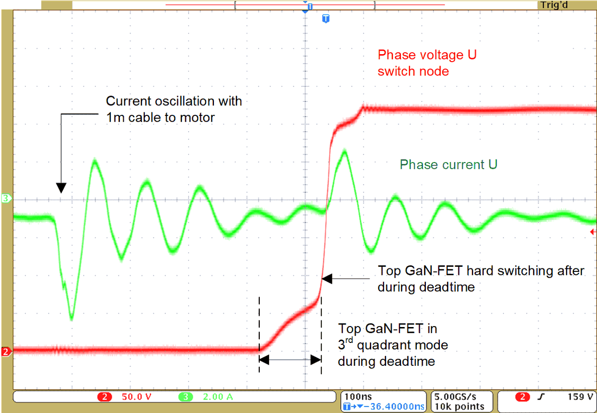 Figure 4-9 Phase U Rising Edge Waveform at –1 A, 1-m Cable to AC Induction Motor
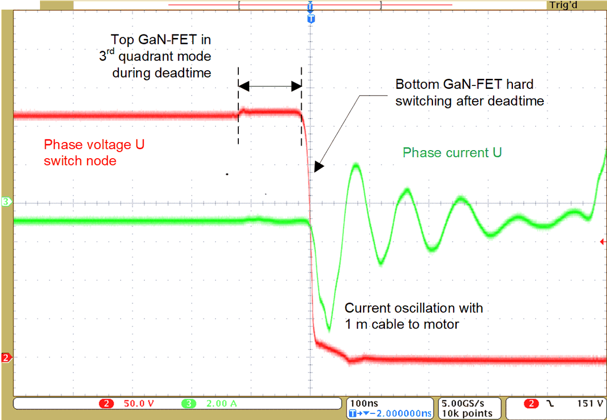 Figure 4-10 Phase U Falling Edge Waveform at –1 A, 1-m Cable to AC Induction Motor
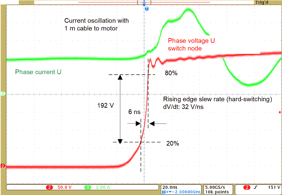 Figure 4-11 Phase U Rising Edge Waveform at 4 A, 1-m Cable to AC Induction Motor
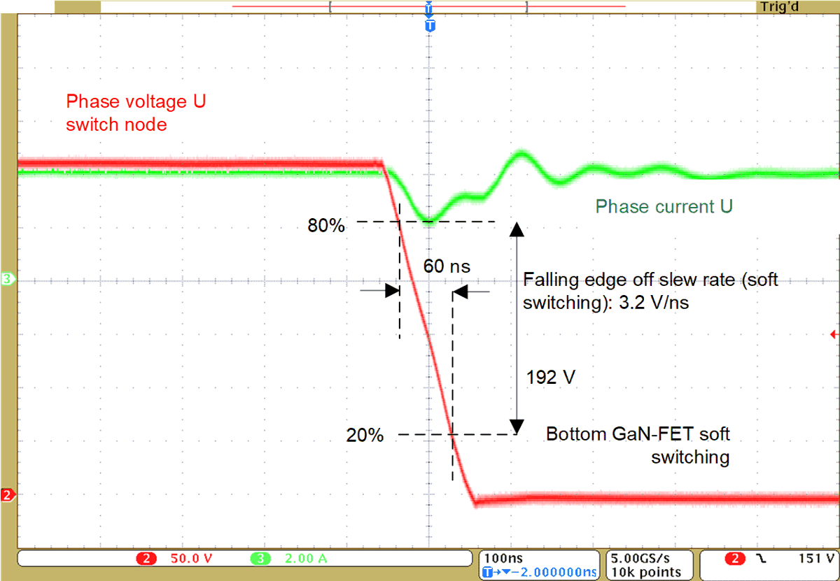 Figure 4-12 Phase U Falling Edge Waveform at 4 A, 1-m Cable to AC Induction Motor
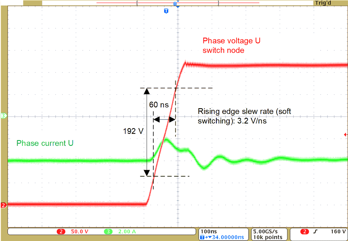 Figure 4-13 Phase U Rising Edge Waveform at –4 A, 1-m Cable to AC Induction Motor
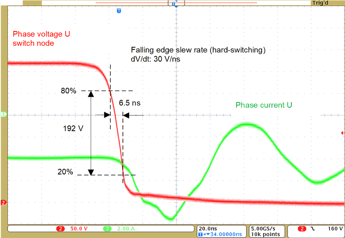 Figure 4-14 Phase U Falling Edge Waveform at –4 A, 1-m Cable to AC Induction Motor
The rising edge slew rate from 20% to 80% in hard-switching mode is around 32 V/ns, the falling edge slew rate from 80% to 20% in hard-switching mode is around 30 V/ns, close to the configured 30 V/ns turn-on slew rate with the LMG3422R030.
Observe that at ±4 A or higher phase currents, the phase current U is large enough to fully discharge (or charge) the effective parasitic output capacitance of the half-bridge during the short dead time, hence the corresponding GaN-FET is soft switching. From the phase voltage drop during soft-switching, the effective output capacitance of each half-bridge can be estimated using Equation 4.
The capacitance COSS,HB is basically the sum of the bottom and top CO(tr) of the GaN-FET and the corresponding parasitic capacitance of the PCB, motor cable, and motor. See the Efficiency Measurements section for further analysis.
The phase current oscillations are mainly due to motor cable and motor windings, a shorter cable leads to lower peak oscillations and higher oscillation frequency, as shown in Figure 4-15 and Figure 4-16. The peak amplitude and frequency of the parasitic oscillations were almost independent of the load current. Compared to the 1-m cable with the AC induction motor, the peak oscillation amplitude during hard-switching reduces by 80% from 5 Apeak to 1 Apeak, the frequency increases from 10 MHz to 40 MHz, while the duration reduces from 500 ns to less than 200 ns.
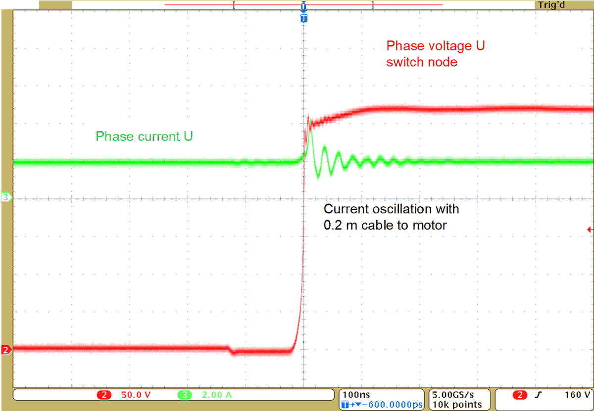 Figure 4-15 Phase U Rising Edge Waveform at 2 A, 0.2-m Cable to PM Synchronous Motor
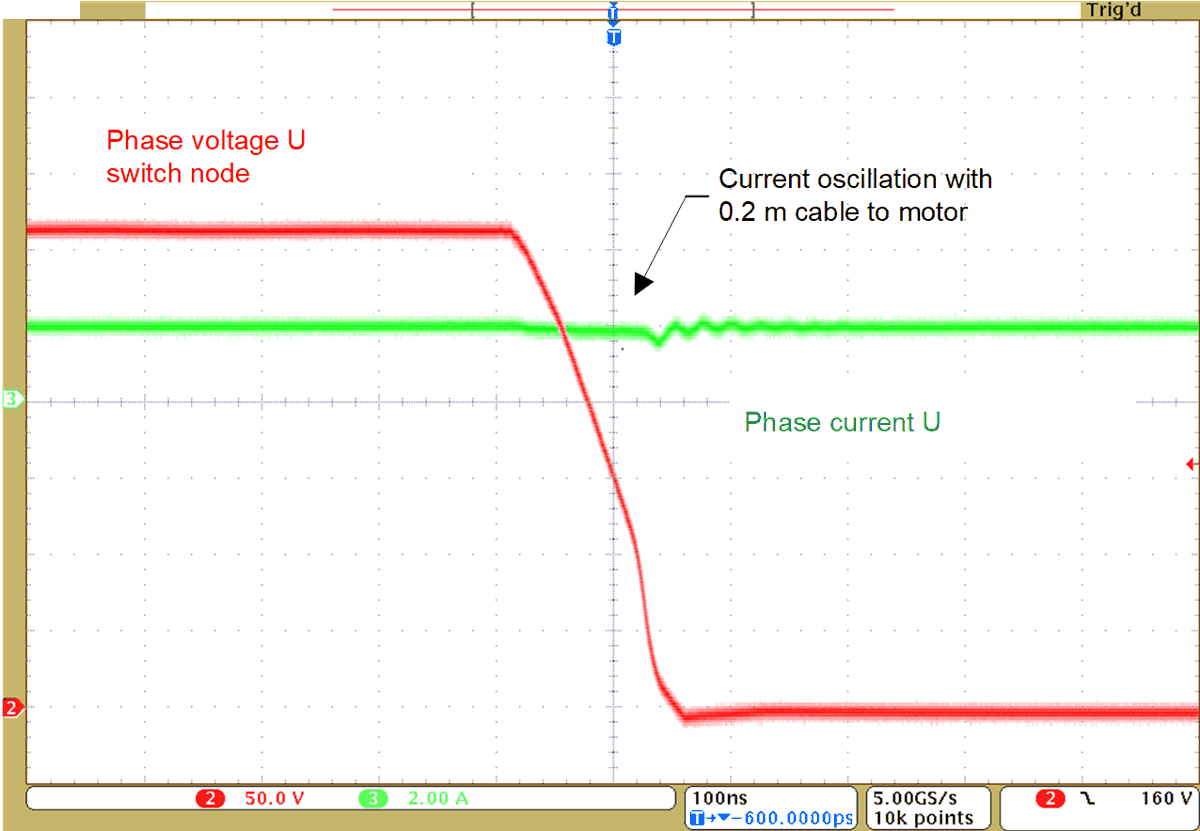 Figure 4-16 Phase U Falling Edge Waveform at 2 A, 0.2-Cable to PM Synchronous Motor