TIDUF28 November   2023


  1.   1
  2.   Description
  3.   Resources
  4.   Features
  5.   Applications
  6.   6
  7. 1System Description
    1. 1.1 Key System Specifications
  8. 2System Overview
    1. 2.1 Block Diagram
    2. 2.2 Highlighted Products
      1. 2.2.1 LMG3422R030
      2. 2.2.2 ISO7741
      3. 2.2.3 AMC1306M05
      4. 2.2.4 AMC1035
      5. 2.2.5 TPSM560R6H
      6. 2.2.6 TPSM82903
  9. 3System Design Theory
    1. 3.1 Power Switches
      1. 3.1.1 GaN-FET Selection Criterion
      2. 3.1.2 HVBUS Decoupling and 12-V Bootstrap Supply
      3. 3.1.3 GaN_FET Turn-on Slew Rate Configuration
      4. 3.1.4 PWM Input Filter and Dead-Time Calculation
      5. 3.1.5 Signal Level Shifting
      6. 3.1.6 LMG3422R030 Fault Reporting
      7. 3.1.7 LMG3422R030 Temperature Monitoring
    2. 3.2 Phase Current Sensing
      1. 3.2.1 Shunt
      2. 3.2.2 AMC1306M05 Analog Input-Filter
      3. 3.2.3 AMC1306M05 Digital Interface
      4. 3.2.4 AMC1306M05 Supply
    3. 3.3 DC-Link (HV_BUS) Voltage Sensing
    4. 3.4 Phase Voltage Sensing
    5. 3.5 Control Supply
    6. 3.6 MCU Interface
  10. 4Hardware, Software, Testing Requirements, and Test Results
    1. 4.1 Hardware Requirements
      1. 4.1.1 PCB
      2. 4.1.2 MCU Interface
    2. 4.2 Software Requirements
    3. 4.3 Test Setup
      1. 4.3.1 Precautions
      2. 4.3.2 Test Procedure
    4. 4.4 Test Results
      1. 4.4.1 24-V Input Control Supply
      2. 4.4.2 Propagation Delay PWM to Phase Voltage Switch Node
      3. 4.4.3 Switch Node Transient at 320-VDC Bus Voltage
      4. 4.4.4 Phase Voltage Linearity and Distortion at 320 VDC and 16-kHz PWM
      5. 4.4.5 Inverter Efficiency and Thermal Characteristic
        1. 4.4.5.1 Efficiency Measurements
        2. 4.4.5.2 Thermal Analysis and SOA Without Heat Sink at 320 VDC and 16-kHz PWM
  11. 5Design and Documentation Support
    1. 5.1 Design Files
      1. 5.1.1 Schematics
      2. 5.1.2 BOM
      3. 5.1.3 PCB Layout Recommendations
        1. 5.1.3.1 Layout Prints
      4. 5.1.4 Altium Project
      5. 5.1.5 Gerber Files
      6. 5.1.6 Assembly Drawings
    2. 5.2 Tools and Software
    3. 5.3 Documentation Support
    4. 5.4 Support Resources
    5. 5.5 Trademarks
  12. 6About the Author

Phase Voltage Sensing

The TIDA-010255 provides an option to sense the three phase voltages with an analog-to-digital converter, typically integrated in the hot-side control MCU. Due to the very low dead-time of the LMG3422R030 GaN-FETs of 100 ns, the phase voltage can accurately be estimated using the PWM duty cycle and the DC-link voltage.

The phase voltage to GND is sensed using a high-voltage resistor divider and a low-pass filter to attenuate the PWM switching frequency. The high-impedance resistor divider R7, R18, R55, and R4 is scaled to provide a 3-V signal at a 480-VDC phase to GND voltage. The low-pass filter R58 and C49 has a cutoff frequency of 360 Hz to attenuate the PWM carrier frequency. Schottky diodes to clamp the maximum voltage at V_PHASE to around 3.6 V are not added intentionally, since the voltage is not supposed to exceed 3 V even during operating conditions with 480-VDC transient DC-link voltage, while the 360-Hz low-pass filter needs to suppress high-frequency transients.
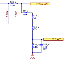
GUID-20231101-SS0I-CLK6-Q4NR-B8NDKN3QM9CX-low.gifFigure 3-9 Phase V to GND Analog Phase Voltage Sensing Schematic