SLUAAA2 March 2021 LM25101 , LM5101A , LM5101B , LM5101C , LM5108 , UCC27200 , UCC27200-Q1 , UCC27201 , UCC27201A , UCC27201A-Q1 , UCC27210 , UCC27211 , UCC27211A , UCC27211A-Q1 , UCC27212 , UCC27212A-Q1 , UCC27282 , UCC27282-Q1 , UCC27284 , UCC27284-Q1 , UCC27288 , UCC27289
1 Understanding and Comparing Peak Current Capability of Gate Drivers
This tech note explains how to evaluate the gate drive strength (peak output current) of different gate drivers, factors affecting the peak source and sink current, and how it affects the performance of the system.
Gate drivers are used to drive power switches such as MOSFET, IGBT, and GaN, mostly in circuits where controllers are not capable of directly driving these power switches due to lack of peak source and sink current. Most gate driver datasheets specify typical drive current capability in a simple manner as shown in table below.
| PARAMETER | CONDITION | MIN | TYP | MAX |
|---|---|---|---|---|
| IPeak pull-up | VO = 0V | 1.6A | ||
| IPeak pull-down | VO = 12V | 1.6A |
This is helpful for general understanding, but comparing two or more gate drivers only based on these typical values may not yield optimum system performance or even optimum cost of the design. It is important to note at what test condition this peak current is specified. Some gate drivers yield higher typical drive current at higher bias voltage. Thus, a gate driver that is specified as 2.5A at 12V cannot be compared directly with a gate driver that specifies 3.5A at 16V. It should also be noted that the switching losses will increase with higher bias voltage, and thus even though the drive current is higher, the system efficiency may reduce.
Power supply design engineers need minimum and maximum values of most parameters across the operating temperature range to optimize their designs. When drive current is specified as a typical value, the RDS(on) of the output stage of the gate driver may be used to estimate drive current variation and may also be used to compare multiple gate drivers. When comparing RDS(on), care should be taken that the test conditions are the same. RDS(on) is either specified directly or can be derived from the output voltage and test current specification as RDS(on) = VO / IO, from the valuse show in the table below. Here it should be noted that only two same types of output structures can be compared this way.
| PARAMETER | CONDITION | MIN | TYP | MAX |
|---|---|---|---|---|
| VOL, Low level output | IO = 100mA | 0.1V | 0.4V | |
| VOH, High level output | IO = 100mA | 0.1V | 0.4V |
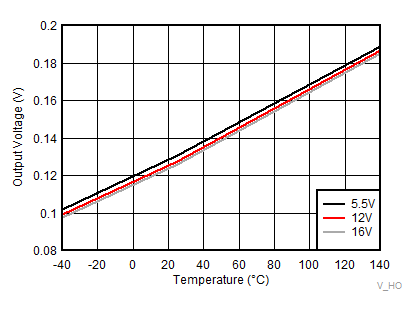
Similar to bias voltage, the ambient temperature also affects the drive current of the gate driver. To understand and optimize the system performance it is also important to evaluate the output voltage variation across bias supply and across temperature. As can be seen from Figure 1, RDS(ON) of the output stage of the UCC27282 does not get affected by bias voltage irrespective of the operating temperature. It means that even at lower bias voltage the drive current capability does not change significantly. Good drive current capability at lower bias voltage results in reduced switching losses and therefore better efficiency.
Psw = Vbias x Qg x Fsw
Where,
Psw = Gate driver switching loss per channel
Qg = Total gate charge of power MOSFET
Fsw = Power stage switching frequency
Good drive strength at lower bias voltage also enables increase in switching frequency of the power stage, which in-turn will reduce the size, weight, and cost of magnetics in the system.
 Figure 1-1 UCC27282 Output Voltage.
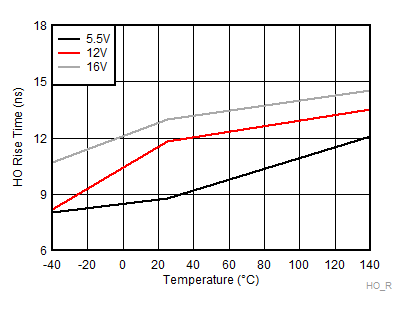
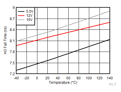
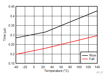
 As mentioned earlier, the primary purpose of the gate driver is, to turn-on and turn-off the power device efficiently. The direct measure of this capability is the rise and fall time specification of the gate driver. Therefore, when comparing multiple gate drivers, it is necessary to compare this specification more so than to compare the typical peak pull-up and pull-down current specification. The test condition needs to be the same for all the gate drivers being compared.
 Figure 1-2 UCC27282 Rise Time (CL=1800pF).
  Figure 1-3 UCC27282 Fall Time (CL=1800pF).
  Figure 1-4 UCC27282 Rise/Fall Time (CL=100nF).
 In summary, design engineers need various factors to compare multiple gate drivers' drive strength. These factors are type of switching power device, gate charge of the power device, external gate resistor, test conditions, bias voltage, and operating temperature.
| Device | Interlock | Enable | Diode | UVLO |
|---|---|---|---|---|
| UCC27282 | Yes | Yes | Yes | 5V |
| UCC27284 | No | Yes | Yes | 5V |
| UCC27288 | No | No | No | 8V |
| UCC27289 | No | No | Yes | 8V |