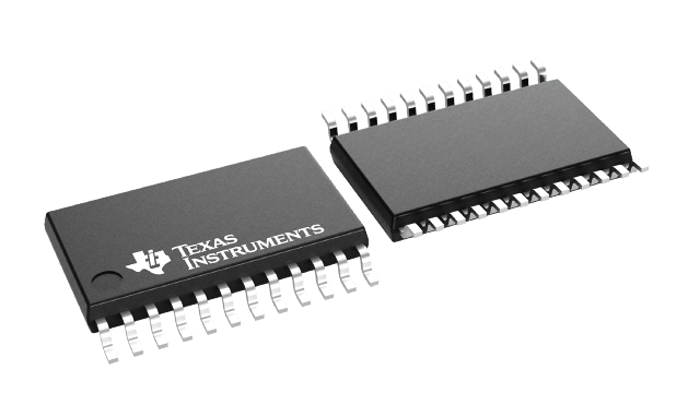
Packaging information
| Package | Pins TSSOP (PW) | 24 |
| Operating temperature range (°C) -40 to 85 |
| Package qty | Carrier 2,000 | LARGE T&R |
Features for the CDCE949
- Member of programmable clock generator family
- CDCEx913: 1 PLL, 3 outputs
- CDCEx925: 2 PLLs, 5 outputs
- CDCEx937: 3 PLLs, 7 outputs
- CDCEx949: 4 PLLs, 9 outputs
- In-system programmability and EEPROM
- Serial programmable volatile register
- Nonvolatile EEPROM to store customer settings
- Flexible input clocking concept
- External crystal: 8MHz to 32MHz
- On-chip VCXO pull-range: ±150ppm
- Single-ended LVCMOS up to 160MHz
- Free selectable output frequency up to 230MHz
- Low-noise PLL core
- PLL loop filter components integrated
- Low period jitter: 60ps (typical)
- Separate output supply pins
- CDCE949: 3.3V and 2.5V
- CDCEL949: 1.8V
- Flexible clock driver
- Three user-definable control inputs [S0/S1/S2] (for example: SSC selection, frequency switching, output enable or power down)
- Generates highly accurate clocks for video, audio, USB, IEEE1394, RFID, Bluetooth, WLAN, Ethernet™, and GPS
- Generates common clock frequencies used with TI-DaVinci™, OMAP™, DSPs
- Programmable SSC modulation
- Enables 0ppm clock generation
- 1.8V device core supply
- Wide temperature range: –40°C to 85°C
- Packaged in TSSOP
- Development and programming kit for easy PLL design and programming (TI Pro-Clock™)
Description for the CDCE949
The CDCE949 and CDCEL949 are modular PLL-based low cost, high-performance, programmable clock synthesizers, multipliers, and dividers. These devices generate up to nine output clocks from a single input frequency. Each output is programmable in-system for any clock frequency up to 230MHz, using up to four independent configurable PLLs.
The CDCEx949 has separate output supply pins (VDDOUT): 1.8V for the CDCEL949 and 2.5V to 3.3V for the CDCE949.
The input accepts an external crystal or LVCMOS clock signal. If an external crystal is used, an on-chip load capacitor is adequate for most applications. The value of the load capacitor is programmable from 0pF to 20pF. Additionally, an on-chip VCXO is selectable, allowing synchronization of the output frequency to an external control signal, that is, a PWM signal.
The deep M/N divider ratio allows the generation of 0ppm audio or video, networking (WLAN, Bluetooth, Ethernet, GPS) or Interface (USB, IEEE1394, Memory Stick) clocks from a reference input frequency, such as 27MHz.
All PLLs support spread spectrum clocking (SSC). SSC can be center-spread or down-spread clocking. This is a common technique to reduce electromagnetic interference (EMI).
Based on the PLL frequency and the divider settings, the internal loop-filter components are automatically adjusted to achieve high stability, and to optimize the jitter-transfer characteristics of each PLL.
The device supports non-volatile EEPROM programming for easy customization of the device to the application. The CDCEx949 is preset to a factory-default configuration. The device can be reprogrammed to a different application configuration before PCB assembly, or reprogrammed by in-system programming. All device settings are programmable through the SDA and SCL bus, a 2-wire serial interface.
