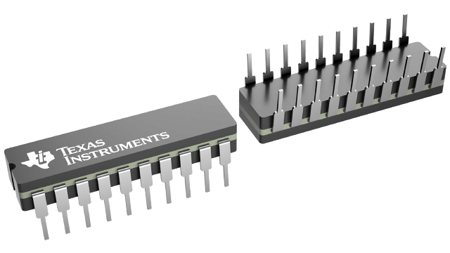
Packaging information
| Package | Pins CDIP (J) | 20 |
| Operating temperature range (°C) -55 to 125 |
| Package qty | Carrier 20 | TUBE |
Features for the SN54HCT240
- Operating voltage range of 4.5V to 5.5V
- High-current outputs drive up to 15 LSTTL loads
- Low power consumption, 80µA max ICC
- Typical tpd = 12 ns
- ±6mA output drive at 5V
- Low input current of 1µA max
- Inputs are TTL-voltage compatible
- 3-state outputs drive bus lines or buffer memory address registers
Description for the SN54HCT240
These octal buffers and line drivers are designed specifically to improve both the performance and density of 3-state memory address drivers, clock drivers, and bus-oriented receivers and transmitters. The ’HCT240 devices are organized as two 4-bit buffers/drivers with separate output-enable (OE) inputs. When OE is low, the device passes inverted data from the A inputs to the Y outputs. When OE is high, the outputs are in the high-impedance state.
