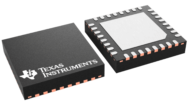
Gehäuseinformationen
| Gehäuse | Pins VQFN (RHB) | 32 |
| Betriebstemperaturbereich (°C) -20 to 85 |
| Gehäusemenge | Träger 250 | SMALL T&R |
Merkmale von TRF7962A
- Completely Integrated Protocol Handling for ISO/IEC 15693 and ISO/IEC 18000-3
- Input Voltage Range: 2.7 VDC to 5.5 VDC
- Programmable Output Power:
+20 dBm (100 mW) or +23 dBm (200 mW) - Programmable I/O Voltage Levels:
1.8 VDC to 5.5 VDC - Programmable System Clock Frequency Output (RF, RF/2, RF/4)
- Programmable Modulation Depth
- Dual Receiver Architecture With RSSI for Elimination of "Read Holes" and Adjacent Reader System or Ambient In-Band Noise Detection
- Programmable Power Modes for Ultra-Low-Power System Design (Power Down <0.5 µA)
- Parallel or SPI Interface
- Integrated Voltage Regulator for Microcontroller Supply
- Temperature Range: –25°C to 85°C
- 32-Pin QFN Package (5 mm × 5 mm) (RHB)
Beschreibung von TRF7962A
The TRF7962A device is an integrated analog front-end (AFE) and data-framing device for a 13.56-MHz RFID reader/writer system that supports ISO/IEC 15693. Built-in programming options make it suitable for a wide range of applications for proximity and vicinity identification systems.
The reader is configured by selecting the desired protocol in the control registers. Direct access to all control registers allows fine tuning of various reader parameters as needed.
The TRF7962A device supports data rates 6 kbps and 26 kbps with all framing and synchronization tasks for the ISO protocols onboard. The device also supports reader/writer mode for NFC Forum tag type 5. NFC Forum tag type 5 is supported with the built-in protocol decoders used in Direct Mode 2. NFC Forum tag type 1 requires the use of Direct Mode 0. Other standards and custom protocols can also be implemented by using Direct Mode 0. Direct Mode 0 lets the user fully control the AFE and also gain access to the raw subcarrier data or the unframed, but already ISO-formatted, data and the associated (extracted) clock signal.
The receiver system has a dual-input receiver architecture to maximize communication robustness. The receivers also include various automatic and manual gain control options. The received signal strength from transponders, ambient sources, or internal levels is available in the RSSI register.
A SPI or parallel interface can be used for the communication between the MCU and the TRF7962A reader. When the built-in hardware encoders and decoders are used, transmit and receive functions use a 12-byte FIFO register. For direct transmit or receive functions, the encoders or decoders can be bypassed so the MCU can process the data in real time.
The TRF7962A device supports a wide supply voltage range of 2.7 V to 5.5 V and data communication levels from 1.8 V to 5.5 V for the MCU I/O interface.
The transmitter has selectable output power levels of 100 mW (+20 dBm) or 200 mW (+23 dBm) equivalent into a 50-Ω load when using a 5-V supply and supports OOK and ASK modulation with selectable modulation depth.
The built-in programmable auxiliary voltage regulator delivers up to 20 mA to supply an MCU and additional external circuits within the reader system.
To evaluate the latest products in the TRF79xx product family – TRF7970A and TRF7964A – see the NFC Transceiver Booster Pack.
Documentation, Tools, Reference Designs, and Software, Samples
