CD4541B

アクティブ

CMOS プログラマブル タイマ - 高電圧タイプ (20V 定格)

製品詳細

Technology family CD4000 Bits (#) 1 Rating Catalog Operating temperature range (°C) -55 to 125
PDIP (N) 14 181.42 mm² (19.3 mm × 9.4 mm) TSSOP (PW) 14 32 mm² (5 mm × 6.4 mm) SOIC (D) 14 51.9 mm² (8.65 mm × 6 mm) SOP (NS) 14 79.56 mm² (10.2 mm × 7.8 mm)
  • Low Symmetrical Output Resistance, Typically 100 at VDD = 15V
  • Built-In Low-Power RC Oscillator
  • Oscillator Frequency Range . . . DC to 100kHz
  • External Clock (Applied to Pin 3) can be Used Instead of Oscillator
  • Operates as 2 N Frequency Divider or as a Single-Transition Timer
  • Q/Q\ Select Provides Output Logic Level Flexibility
  • AUTO or MASTER RESET Disables Oscillator During Reset to Reduce Power Dissipation
  • Operates With Very Slow Clock Rise and Fall Times
  • Capable of Driving Six Low Power TTL Loads, Three Low-Power Schottky Loads, or Six HTL Loads Over the Rated Temperature Range
  • Symmetrical Output Characteristics
  • 100% Tested for Quiescent Current at 20V
  • 5V, 10V, and 15V Parametric Ratings
  • Meets All Requirements of JEDEC Standard No. 13B, "Standard Specifications for Description of ’B’ Series CMOS Devices"

Data sheet acquired from Harris Semiconductor

  • Low Symmetrical Output Resistance, Typically 100 at VDD = 15V
  • Built-In Low-Power RC Oscillator
  • Oscillator Frequency Range . . . DC to 100kHz
  • External Clock (Applied to Pin 3) can be Used Instead of Oscillator
  • Operates as 2 N Frequency Divider or as a Single-Transition Timer
  • Q/Q\ Select Provides Output Logic Level Flexibility
  • AUTO or MASTER RESET Disables Oscillator During Reset to Reduce Power Dissipation
  • Operates With Very Slow Clock Rise and Fall Times
  • Capable of Driving Six Low Power TTL Loads, Three Low-Power Schottky Loads, or Six HTL Loads Over the Rated Temperature Range
  • Symmetrical Output Characteristics
  • 100% Tested for Quiescent Current at 20V
  • 5V, 10V, and 15V Parametric Ratings
  • Meets All Requirements of JEDEC Standard No. 13B, "Standard Specifications for Description of ’B’ Series CMOS Devices"

Data sheet acquired from Harris Semiconductor

CD4541B programmable timer consists of a 16-stage binary counter, an oscillator that is controlled by external R-C components (2 resistors and a capacitor), an automatic power-on reset circuit, and output control logic. The counter increments on positive-edge clock transitions and can also be reset via the MASTER RESET input.

The output from this timer is the Q or Q\ output from the 8th, 10th, 13th, or 16th counter stage. The desired stage is chosen using time-select inputs A and B (see Frequency Select Table).

The output is available in either of two modes selectable via the MODE input, pin 10 (see Truth Table). When this MODE input is a logic "1", the output will be a continuous square wave having a frequency equal to the oscillator frequency divided by 2N. With the MODE input set to logic "0" and after a MASTER RESET is initiated, the output (assuming Q output has been selected) changes from a low to a high state after 2N-1 counts and remains in that state until another MASTER RESET pulse is applied or the MODE input is set to a logic "1".

Timing is initialized by setting the AUTO RESET input (pin 5) to logic "0" and turning power on. If pin 5 is set to logic "1", the AUTO RESET circuit is disabled and counting will not start until after a positive MASTER RESET pulse is applied and returns to a low level. The AUTO RESET consumes an appreciable amount of power and should not be used if low-power operation is desired. For reliable automatic power-on reset, VDD should be greater than 5V.

The RC oscillator, shown in Figure 2, oscillates with a frequency determined by the RC network and is calculated using:
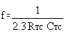
Where f is between 1kHz and 100kHz and RS and 2RTC.

CD4541B programmable timer consists of a 16-stage binary counter, an oscillator that is controlled by external R-C components (2 resistors and a capacitor), an automatic power-on reset circuit, and output control logic. The counter increments on positive-edge clock transitions and can also be reset via the MASTER RESET input.

The output from this timer is the Q or Q\ output from the 8th, 10th, 13th, or 16th counter stage. The desired stage is chosen using time-select inputs A and B (see Frequency Select Table).

The output is available in either of two modes selectable via the MODE input, pin 10 (see Truth Table). When this MODE input is a logic "1", the output will be a continuous square wave having a frequency equal to the oscillator frequency divided by 2N. With the MODE input set to logic "0" and after a MASTER RESET is initiated, the output (assuming Q output has been selected) changes from a low to a high state after 2N-1 counts and remains in that state until another MASTER RESET pulse is applied or the MODE input is set to a logic "1".

Timing is initialized by setting the AUTO RESET input (pin 5) to logic "0" and turning power on. If pin 5 is set to logic "1", the AUTO RESET circuit is disabled and counting will not start until after a positive MASTER RESET pulse is applied and returns to a low level. The AUTO RESET consumes an appreciable amount of power and should not be used if low-power operation is desired. For reliable automatic power-on reset, VDD should be greater than 5V.

The RC oscillator, shown in Figure 2, oscillates with a frequency determined by the RC network and is calculated using:

Where f is between 1kHz and 100kHz and RS and 2RTC.

ダウンロード 字幕付きのビデオを表示 ビデオ

お客様が関心を持ちそうな類似品

open-in-new 代替品と比較
比較対象デバイスと類似の機能。
TPL5010 アクティブ ウォッチドッグ機能と手動リセット機能搭載、ナノパワー システム タイマ Watchdog timer

技術資料

結果が見つかりませんでした。検索条件をクリアしてから、再度検索を試してください。
1 をすべて表示
上位の文書 タイプ タイトル フォーマットオプション 最新の英語版をダウンロード 日付
* データシート CD4541B データシート (Rev. E) 2003/08/21

設計と開発

その他のアイテムや必要なリソースを参照するには、以下のタイトルをクリックして詳細ページをご覧ください。

評価ボード

14-24-LOGIC-EVM — 14 ピンから 24 ピンの D、DB、DGV、DW、DYY、NS、PW の各パッケージに封止した各種ロジック製品向けの汎用評価基板

14-24-LOGIC-EVM 評価基板 (EVM) は、14 ピンから 24 ピンの D、DW、DB、NS、PW、DYY、DGV の各パッケージに封止した各種ロジック デバイスをサポートする設計を採用しています。

ユーザー ガイド: PDF | HTML
サポート対象の製品とハードウェア
在庫あり
制限:
??asset.out-of-stock-ti_ja_JP??
入手不可
パッケージ ピン数 CAD シンボル、フットプリント、および 3D モデル
PDIP (N) 14 Ultra Librarian
TSSOP (PW) 14 Ultra Librarian
SOIC (D) 14 Ultra Librarian
SOP (NS) 14 Ultra Librarian

購入と品質

サポートとトレーニング

TI E2E™ フォーラムでは、TI のエンジニアからの技術サポートを提供

コンテンツは、TI 投稿者やコミュニティ投稿者によって「現状のまま」提供されるもので、TI による仕様の追加を意図するものではありません。使用条件をご確認ください。

TI 製品の品質、パッケージ、ご注文に関するお問い合わせは、TI サポートをご覧ください。​​​​​​​​​​​​​​

ビデオ