SN65LVDT32B
- Meets or Exceeds the Requirements of ANSI EIA/TIA-644 Standard for Signaling Rates(1) up to 400 Mbps
- Operates With a Single 3.3-V Supply
- -2-V to 4.4-V Common-Mode Input Voltage Range
- Differential Input Thresholds <50 mV With 50 mV of Hysteresis Over Entire Common-
Mode Input Voltage Range - Integrated 110-
 Line Termination Resistors Offered With the LVDT Series
 - Propagation Delay Times 4 ns (typ)
- Active Fail Safe Assures a High-Level Output With No Input
- Bus-Pin ESD Protection Exceeds 15 kV—HBM
- Inputs Remain High-Impedance on Power Down
- Recommended Maximum Parallel Rate of 200 M-Transfer/s
- Available in Small-Outline Package With 1,27-mm Terminal Pitch
- Pin-Compatible With the AM26LS32, MC3486, or µA9637
(1) Signaling rate, 1/t, where t is the minimum unit interval and is expressed in the units bit/s (bits per second).
This family of differential line receivers offers improved performance and features that implement the electrical characteristics of low-voltage differential signaling (LVDS). LVDS is defined in the TIA/EIA-644 standard. This improved performance represents the second generation of receiver products for this standard, providing a better overall solution for the cabled environment. This generation of products is an extension to TI's overall product portfolio and is not necessarily a replacement for older LVDS receivers.
Improved features include an input common-mode voltage range 2 V wider than the minimum required by the standard. This will allow longer cable lengths by tripling the allowable ground noise tolerance to 3 V between a driver and receiver. TI has additionally introduced an even wider input common-mode voltage range of -4 to 5 V in their SN65LVDS/T33 and SN65LVDS/T34.
Precise control of the differential input voltage thresholds now allows for inclusion of 50 mV of input voltage hysteresis to improve noise rejection on slowly changing input signals. The input thresholds are still no more than ±50 mV over the full input common-mode voltage range.
The high-speed switching of LVDS signals almost always necessitates the use of a line impedance matching resistor at the receiving-end of the cable or transmission media. The SN65LVDT series of receivers eliminates this external resistor by integrating it with the receiver. The non-terminated SN65LVDS series is also available for multidrop or other termination circuits.
The receivers can withstand ±15-kV human-body model (HBM) and ±600 V-machine model (MM) electrostatic discharges to the receiver input pins with respect to ground without damage. This provides reliability in cabled and other connections where potentially damaging noise is always a threat.
The receivers also include a (patent pending) fail-safe circuit that will provide a high-level output within 600 ns after loss of the input signal. The most common causes of signal loss are disconnected cables, shorted lines, or powered-down transmitters. This prevents noise from being received as valid data under these fault conditions. This feature may also be used for wired-OR bus signaling.
The intended application of these devices and signaling technique is for point-to-point baseband data transmission over controlled impedance media of approximately 100 . The transmission media may be printed-circuit board traces, backplanes, or cables. The ultimate rate and distance of data transfer is dependent upon the attenuation characteristics of the media and the noise coupling to the environment.
The SN65LVDS32B, SN65LVDT32B, SN65LVDS3486B, SN65LVDT3486B, SN65LVDS9637B, and SN65LVDT9637B are characterized for operation from -40°C to 85°C.
您可能會感興趣的類似產品
針腳對針腳的功能與所比較的裝置相同。
技術文件
| 重要文件 | 類型 | 標題 | 格式選項 | 下載最新的英文版本 | 日期 | |
|---|---|---|---|---|---|---|
| * | 資料表 | High-Speed Differential Receivers datasheet (Rev. B) | 2007/4/23 | |||
| Application brief | LVDS to Improve EMC in Motor Drives | 2018/9/27 | ||||
| Application brief | How Far, How Fast Can You Operate LVDS Drivers and Receivers? | 2018/8/3 | ||||
| Application brief | How to Terminate LVDS Connections with DC and AC Coupling | 2018/5/16 | ||||
| 應用說明 | An Overview of LVDS Technology | 1998/10/5 |
設計與開發
如需其他條款或必要資源,請按一下下方的任何標題以檢視詳細頁面 (如有)。
SN65LVDS31-32BEVM — 適用 LVDS31 和 LVDS32B 的 SN65LVDS31-32B 低電壓差動訊號評估模組
TI offers a series of low-voltage differential signaling (LVDS) evaluation modules (EVMs) designed for analysis of the electrical characteristics of LVDS drivers and receivers. Four unique EVMs are available to evaluate the different classes of LVDS devices offered by TI.
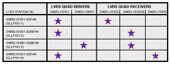
As seen (...)
| 封裝 | 針腳 | CAD 符號、佔位空間與 3D 模型 |
|---|---|---|
| SOIC (D) | 16 | Ultra Librarian |