SNAS787A November 2019 – February 2020 CDCDB2000
PRODUCTION DATA.
- 1 Features
- 2 Applications
- 3 Description
- 4 Revision History
- 5 Pin Configuration and Functions
- 6 Specifications
-
7 Detailed Description
- 7.1 Overview
- 7.2 Functional Block Diagram
- 7.3 Feature Description
- 7.4 Device Functional Modes
- 7.5 Programming
- 7.6
Register Maps
- 7.6.1
CDCDB2000 Registers
- 7.6.1.1 OECR1 Register (Address = 0h) [reset = 78h]
- 7.6.1.2 OECR2 Register (Address = 1h) [reset = FFh]
- 7.6.1.3 OECR3 Register (Address = 2h) [reset = FFh]
- 7.6.1.4 OERDBK Register (Address = 3h) [reset = 0h]
- 7.6.1.5 SBRDBK Register (Address = 4h) [reset = 1h]
- 7.6.1.6 VDRREVID Register (Address = 5h) [reset = X]
- 7.6.1.7 DEVID Register (Address = 6h) [reset = X]
- 7.6.1.8 BTRDCNT Register (Address = 7h) [reset = 8h]
- 7.6.1.9 SBIMSK1 Register (Address = 8h) [reset = 0h]
- 7.6.1.10 SBIMSK2 Register (Address = 9h) [reset = 0h]
- 7.6.1.11 SBIMSK3 Register (Address = Ah) [reset = 0h]
- 7.6.1
CDCDB2000 Registers
- 8 Application and Implementation
- 9 Power Supply Recommendations
- 10Layout
- 11Device and Documentation Support
- 12Mechanical, Packaging, and Orderable Information
Package Options
Mechanical Data (Package|Pins)
- NPP|80
Thermal pad, mechanical data (Package|Pins)
Orderable Information
Table 6. Timing Requirements
VDD, VDD_A = 3.3 V ± 5 %, -40 °C < TA < 85 °C. Typical values are at VDD = VDD_A = 3.3 V, 25 °C (unless otherwise noted)| MIN | NOM | MAX | UNIT | |||
|---|---|---|---|---|---|---|
| SMBUS-COMPATIBLE INTERFACE TIMING | ||||||
| fSMB | SMBus operating frequency | 10 | 100 | kHz | ||
| tBUF | Bus free time between STOP and START | 4.7 | µs | |||
| tHD_STA | START condition hold time | 4 | ||||
| tSU_STA | START condition setup time | 4.7 | ||||
| tSU_STO | STOP condition setup time | 4 | ||||
| tHD_DAT | SMBDAT hold time | 300 | ns | |||
| tSU_DAT | SMBDAT setup time | 250 | ||||
| tTIMEOUT | Detect SMBCLK low timeout | 25 | 35 | ms | ||
| tLOW | SMBCLK low period | 4.7 | µs | |||
| tHIGH | SMBCLK high period | 4 | 50 | |||
| tLOW_SL | Cumulative clock low extend time | 25 | ms | |||
| tF | SMBCLK/SMBDAT fall time(1) | 300 | ns | |||
| tR | SMBCLK/SMBDAT rise time(2) | 1000 | ||||
| SIDE-BAND INTERFACE TIMING | ||||||
| tPERIOD | Clock period | 40 | ns | |||
| tSETUP | Setup time to clock | 25 | ||||
| tDSU | Data set up time | 10 | ||||
| tDHOLD | Data hold time | 5 | ||||
| tDELAY | Delay time | 25 | ||||
| tPDLY | Propagation delay | 4 | 10 | CLK periods | ||
| tSLEW | Clock slew rate | 20% - 80% | 0.2 | 3 | V/ns | |
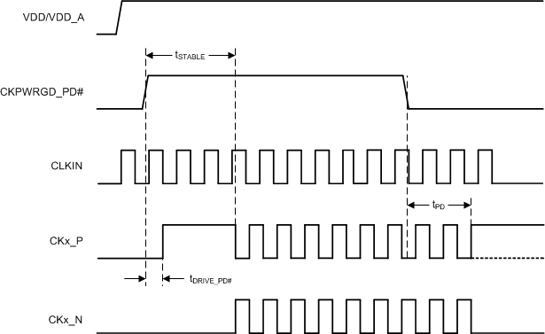
 Figure 1. Start-Up With CLKIN Timing Diagram
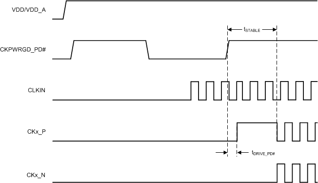
  Figure 2. Start-Up Without CLKIN Timing Diagram
  Figure 3. SMBus Timing Diagram
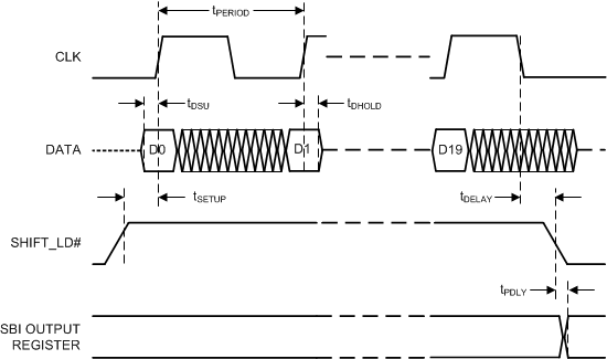
  Figure 4. Side-Band Interface Timing Diagram