SLVSGV9 august   2023 DRV8213

PRODUCTION DATA  

  1.   1
  2. Features
  3. Applications
  4. Description
  5. Revision History
  6. Device Comparison
  7. Pin Configuration and Functions
  8. Specifications
    1. 7.1 Absolute Maximum Ratings
    2. 7.2 ESD Ratings
    3. 7.3 Recommended Operating Conditions
    4. 7.4 Thermal Information
    5. 7.5 Electrical Characteristics
    6. 7.6 Timing Diagrams
    7. 7.7 Typical Operating Characteristics
  9. Detailed Description
    1. 8.1 Overview
    2. 8.2 Functional Block Diagram
    3. 8.3 External Components
    4. 8.4 Feature Description
      1. 8.4.1 Bridge Control
      2. 8.4.2 Current Sense and Regulation (IPROPI)
        1. 8.4.2.1 Current Sensing and Current Mirror Gain Selection
        2. 8.4.2.2 Current Regulation
      3. 8.4.3 Hardware Stall Detection
      4. 8.4.4 Protection Circuits
        1. 8.4.4.1 Overcurrent Protection (OCP)
        2. 8.4.4.2 Thermal Shutdown (TSD)
        3. 8.4.4.3 VM Undervoltage Lockout (UVLO)
    5. 8.5 Device Functional Modes
      1. 8.5.1 Active Mode
      2. 8.5.2 Low-Power Sleep Mode
      3. 8.5.3 Fault Mode
    6. 8.6 Pin Diagrams
      1. 8.6.1 Logic-Level Inputs
      2. 8.6.2 Tri-Level Input
  10. Application and Implementation
    1. 9.1 Application Information
    2. 9.2 Typical Application
      1. 9.2.1 Brushed DC Motor
        1. 9.2.1.1 Design Requirements
        2. 9.2.1.2 Detailed Design Procedure
          1. 9.2.1.2.1 Motor Voltage
          2. 9.2.1.2.2 Motor Current
        3. 9.2.1.3 Stall Detection
          1. 9.2.1.3.1 Detailed Design Procedure
            1. 9.2.1.3.1.1 Hardware Stall Detection Application Description
              1. 9.2.1.3.1.1.1 Hardware Stall Detection Timing
              2. 9.2.1.3.1.1.2 Hardware Stall Threshold Selection
            2. 9.2.1.3.1.2 Software Stall Detection Application Description
              1. 9.2.1.3.1.2.1 Software Stall Detection Timing
              2. 9.2.1.3.1.2.2 Software Stall Threshold Selection
        4. 9.2.1.4 Application Curves
        5. 9.2.1.5 Thermal Performance
          1. 9.2.1.5.1 Steady-State Thermal Performance
          2. 9.2.1.5.2 Transient Thermal Performance
  11. 10Power Supply Recommendations
    1. 10.1 Bulk Capacitance
  12. 11Layout
    1. 11.1 Layout Guidelines
  13. 12Device and Documentation Support
    1. 12.1 Documentation Support
      1. 12.1.1 Related Documentation
    2. 12.2 Receiving Notification of Documentation Updates
    3. 12.3 Community Resources
    4. 12.4 Trademarks
  14. 13Mechanical, Packaging, and Orderable Information
    1. 13.1 Tape and Reel Information

Package Options

Mechanical Data (Package|Pins)
Thermal pad, mechanical data (Package|Pins)
Orderable Information

Overcurrent Protection (OCP)

An analog current limit circuit on each FET limits the current through the FET by limiting the gate drive internally. If this analog current limit persists for longer than the OCP deglitch time (tOCP), all FETs in the H-bridge will disable and nFAULT is pulled low. The driver re-enables after the fault retry period (tRETRY) has passed. If the fault condition is still present, the cycle repeats as shown in Figure 8-11.
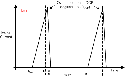
GUID-DA7A44B7-FCB2-46CF-A7FE-2BEA308C9942-low.gifFigure 8-11 OCP Operation

Overcurrent conditions are detected independently on both high- and low-side FETs. This means that a short to ground, supply, or across the motor winding will all result in an overcurrent shutdown. Overcurrent protection does not use the current sense circuitry used for current regulation, so it functions regardless of VREF and IPROPI settings.