SNVS952F December 2012 – May 2021 LM25019
PRODUCTION DATA
- 1 Features
- 2 Applications
- 3 Description
- 4 Revision History
- 5 Pin Configuration and Functions
- 6 Specifications
-
7 Detailed Description
- 7.1 Overview
- 7.2 Functional Block Diagram
- 7.3
Feature Description
- 7.3.1 Control Overview
- 7.3.2 VCC Regulator
- 7.3.3 Regulation Comparator
- 7.3.4 Overvoltage Comparator
- 7.3.5 On-Time Generator
- 7.3.6 Current Limit
- 7.3.7 N-Channel Buck Switch and Driver
- 7.3.8 Synchronous Rectifier
- 7.3.9 Undervoltage Detector
- 7.3.10 Thermal Protection
- 7.3.11 Ripple Configuration
- 7.3.12 Soft Start
- 7.4 Device Functional Modes
- 8 Application and Implementation
- 9 Power Supply Recommendations
- 10Layout
- 11Device and Documentation Support
- 12Mechanical, Packaging, and Orderable Information
Package Options
Mechanical Data (Package|Pins)
Thermal pad, mechanical data (Package|Pins)
- DDA|8
Orderable Information
8.2.2.2 Frequency Selection
At the minimum input voltage, the maximum switching frequency of the LM25019 is restricted by the forced minimum off-time (TOFF(MIN)) as shown in Equation 10.
Equation 10. 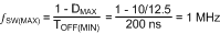
Similarly, at maximum input voltage, the maximum switching frequency of the LM25019 is restricted by the minimum TON as shown in Equation 11.
Equation 11. 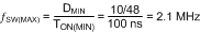
Resistor RON sets the nominal switching frequency based on Equation 12.
Equation 12. 
where
- K = 9 x 10–11
Operation at high switching frequency results in lower efficiency while providing the smallest solution. Using
440 kHz as the target swtiching frequency, the calculated valued of RON is 253 kΩ. The standard value for RON = R3 = 237 kΩ is selected.