SNVS952F December 2012 – May 2021 LM25019
PRODUCTION DATA
- 1 Features
- 2 Applications
- 3 Description
- 4 Revision History
- 5 Pin Configuration and Functions
- 6 Specifications
-
7 Detailed Description
- 7.1 Overview
- 7.2 Functional Block Diagram
- 7.3
Feature Description
- 7.3.1 Control Overview
- 7.3.2 VCC Regulator
- 7.3.3 Regulation Comparator
- 7.3.4 Overvoltage Comparator
- 7.3.5 On-Time Generator
- 7.3.6 Current Limit
- 7.3.7 N-Channel Buck Switch and Driver
- 7.3.8 Synchronous Rectifier
- 7.3.9 Undervoltage Detector
- 7.3.10 Thermal Protection
- 7.3.11 Ripple Configuration
- 7.3.12 Soft Start
- 7.4 Device Functional Modes
- 8 Application and Implementation
- 9 Power Supply Recommendations
- 10Layout
- 11Device and Documentation Support
- 12Mechanical, Packaging, and Orderable Information
Package Options
Mechanical Data (Package|Pins)
Thermal pad, mechanical data (Package|Pins)
- DDA|8
Orderable Information
7.3.1 Control Overview
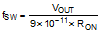
The LM25019 buck regulator employs a control principle based on a comparator and a one-shot on-timer, with the output voltage feedback (FB) compared to an internal reference (1.225 V). If the FB voltage is below the reference, the internal buck switch is turned on for the one-shot timer period, which is a function of the input voltage and the programming resistor (RON). Following the on-time, the switch remains off until the FB voltage falls below the reference, but never before the minimum off-time forced by the minimum off-time one-shot timer. When the FB pin voltage falls below the reference and the minimum off-time one-shot period expires, the buck switch is turned on for another on-time one-shot period. This continues until regulation is achieved and the FB voltage is approximately equal to 1.225 V (typ).
In a synchronous buck converter, the low-side (sync) FET is on when the high-side (buck) FET is off. The inductor current ramps up when the high-side switch is on and ramps down when the high-side switch is off. There is no diode emulation feature in this IC, and therefore, the inductor current can ramp in the negative direction at light load. This causes the converter to operate in continuous conduction mode (CCM) regardless of the output loading. The operating frequency remains relatively constant with load and line variations. The operating frequency can be calculated as shown in Equation 1.
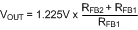
The output voltage (VOUT) is set by two external resistors (RFB1, RFB2). The regulated output voltage is calculated as shown in Equation 2.
This regulator regulates the output voltage based on ripple voltage at the feedback input, requiring a minimum amount of ESR for the output capacitor (COUT). A minimum of 25 mV of ripple voltage at the feedback pin (FB) is required for the LM25019. In cases where the capacitor ESR is too small, additional series resistance can be required (RC in Figure 7-2).
For applications where lower output voltage ripple is required the output can be taken directly from a low ESR output capacitor, as shown in Figure 7-2. However, RC slightly degrades the load regulation.
 Figure 7-2 Low Ripple Output Configuration