SNVS952F December 2012 – May 2021 LM25019
PRODUCTION DATA
- 1 Features
- 2 Applications
- 3 Description
- 4 Revision History
- 5 Pin Configuration and Functions
- 6 Specifications
-
7 Detailed Description
- 7.1 Overview
- 7.2 Functional Block Diagram
- 7.3
Feature Description
- 7.3.1 Control Overview
- 7.3.2 VCC Regulator
- 7.3.3 Regulation Comparator
- 7.3.4 Overvoltage Comparator
- 7.3.5 On-Time Generator
- 7.3.6 Current Limit
- 7.3.7 N-Channel Buck Switch and Driver
- 7.3.8 Synchronous Rectifier
- 7.3.9 Undervoltage Detector
- 7.3.10 Thermal Protection
- 7.3.11 Ripple Configuration
- 7.3.12 Soft Start
- 7.4 Device Functional Modes
- 8 Application and Implementation
- 9 Power Supply Recommendations
- 10Layout
- 11Device and Documentation Support
- 12Mechanical, Packaging, and Orderable Information
Package Options
Mechanical Data (Package|Pins)
Thermal pad, mechanical data (Package|Pins)
- DDA|8
Orderable Information
8.2 Typical Application
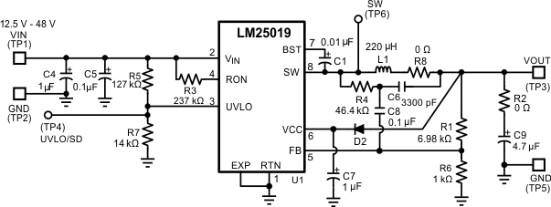
The application schematic of a buck supply is shown in Figure 8-1. For output voltage (VOUT) more than one diode drop higher than the maximum regulation voltage of VCC (8.55 V, see the Section 6.5), the VCC pin can be connected to VOUT through a diode (D2), as shown in Figure 8-1, to improve efficiency and reduce power dissipation in the IC.
The design example shown in Figure 8-1 uses equations from the Section 7.3 with component names provided in the Figure 3-1 schematic. Corresponding component designators from Figure 8-1 are also provided for each selected value.
 Figure 8-1 Final Schematic for 12.5-V to 48-V Input, and 10-V, 100-mA Output Buck Converter