SNVS952F December 2012 – May 2021 LM25019
PRODUCTION DATA
- 1 Features
- 2 Applications
- 3 Description
- 4 Revision History
- 5 Pin Configuration and Functions
- 6 Specifications
-
7 Detailed Description
- 7.1 Overview
- 7.2 Functional Block Diagram
- 7.3
Feature Description
- 7.3.1 Control Overview
- 7.3.2 VCC Regulator
- 7.3.3 Regulation Comparator
- 7.3.4 Overvoltage Comparator
- 7.3.5 On-Time Generator
- 7.3.6 Current Limit
- 7.3.7 N-Channel Buck Switch and Driver
- 7.3.8 Synchronous Rectifier
- 7.3.9 Undervoltage Detector
- 7.3.10 Thermal Protection
- 7.3.11 Ripple Configuration
- 7.3.12 Soft Start
- 7.4 Device Functional Modes
- 8 Application and Implementation
- 9 Power Supply Recommendations
- 10Layout
- 11Device and Documentation Support
- 12Mechanical, Packaging, and Orderable Information
Package Options
Mechanical Data (Package|Pins)
Thermal pad, mechanical data (Package|Pins)
- DDA|8
Orderable Information
8.2.2.5 Type III Ripple Circuit
Type III ripple circuit as described in the Section 7.3.11 section is chosen for this example. For a constant on-time converter to be stable, the injected in-phase ripple must be larger than the capacitive ripple on COUT.
Using type III ripple circuit equations, the target ripple must be greater than the capacitive ripple generated at the primary output.
Cr = C6 = 3300 pF
Cac = C8 = 100 nF
For TON, refer to Equation 3.
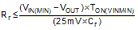
Ripple resistor Rr is
calculated to be 57.6 kΩ. This value provides the minimum ripple for stable
operation. A smaller resistance should be selected to allow for variations in
TON, COUT, and other components. Rr = R4 =
46.4 kΩ is selected for this example application.