SNVS952F December 2012 – May 2021 LM25019
PRODUCTION DATA
- 1 Features
- 2 Applications
- 3 Description
- 4 Revision History
- 5 Pin Configuration and Functions
- 6 Specifications
-
7 Detailed Description
- 7.1 Overview
- 7.2 Functional Block Diagram
- 7.3
Feature Description
- 7.3.1 Control Overview
- 7.3.2 VCC Regulator
- 7.3.3 Regulation Comparator
- 7.3.4 Overvoltage Comparator
- 7.3.5 On-Time Generator
- 7.3.6 Current Limit
- 7.3.7 N-Channel Buck Switch and Driver
- 7.3.8 Synchronous Rectifier
- 7.3.9 Undervoltage Detector
- 7.3.10 Thermal Protection
- 7.3.11 Ripple Configuration
- 7.3.12 Soft Start
- 7.4 Device Functional Modes
- 8 Application and Implementation
- 9 Power Supply Recommendations
- 10Layout
- 11Device and Documentation Support
- 12Mechanical, Packaging, and Orderable Information
Package Options
Mechanical Data (Package|Pins)
Thermal pad, mechanical data (Package|Pins)
- DDA|8
Orderable Information
8.2.2.3 Inductor Selection
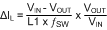
The inductance selection is a compromise between solution size, output ripple, and efficiency. The peak inductor current at maximum load current must be smaller than the minimum current limit of 150 mA. The maximum permissible peak to peak inductor ripple is determined by Equation 13.
The minimum inductance is determined by Equation 14.
Using the maximum VIN of 48 V, the calculation from Equation 14 results in L = 179 μH. A standard value of 220 μH is selected. For proper operation, the inductor saturation current must be higher than the peak current encountered in the application. For robust short circuit protection, the inductor saturation current must be higher than the maximum current limit of 300 mA.