SLASEC8C February 2017 – February 2023 PGA460-Q1
PRODUCTION DATA
- 1 Features
- 2 Applications
- 3 Description
- 4 Revision History
- 5 Pin Configuration and Functions
-
6 Specifications
- 6.1 Absolute Maximum Ratings
- 6.2 ESD Ratings
- 6.3 Recommended Operating Conditions
- 6.4 Thermal Information
- 6.5 Internal Supply Regulators Characteristics
- 6.6 Transducer Driver Characteristics
- 6.7 Transducer Receiver Characteristics
- 6.8 Analog to Digital Converter Characteristics
- 6.9 Digital Signal Processing Characteristics
- 6.10 Temperature Sensor Characteristics
- 6.11 High-Voltage I/O Characteristics
- 6.12 Digital I/O Characteristics
- 6.13 EEPROM Characteristics
- 6.14 Timing Requirements
- 6.15 Switching Characteristics
- 6.16 Typical Characteristics
-
7 Detailed Description
- 7.1 Overview
- 7.2 Functional Block Diagram
- 7.3
Feature Description
- 7.3.1 Power-Supply Block
- 7.3.2 Burst Generation
- 7.3.3 Analog Front-End
- 7.3.4 Digital Signal Processing
- 7.3.5 System Diagnostics
- 7.3.6
Interface Description
- 7.3.6.1 Time-Command Interface
- 7.3.6.2
USART Interface
- 7.3.6.2.1 USART Asynchronous Mode
- 7.3.6.2.2 One-Wire UART Interface
- 7.3.6.2.3 Ultrasonic Object Detection Through UART Operations
- 7.3.6.3 In-System IO-Pin Interface Selection
- 7.3.7 Echo Data Dump
- 7.3.8 Low-Power Mode
- 7.3.9 Transducer Time and Temperature Decoupling
- 7.3.10 Memory CRC Calculation
- 7.3.11 Temperature Sensor and Temperature Data-Path
- 7.3.12 TEST Pin Functionality
- 7.4 Device Functional Modes
- 7.5 Programming
- 7.6 Register Maps
- 8 Application and Implementation
- 9 Device and Documentation Support
- 10Mechanical, Packaging, and Orderable Information
Package Options
Mechanical Data (Package|Pins)
- PW|16
Thermal pad, mechanical data (Package|Pins)
Orderable Information
7.3.3 Analog Front-End
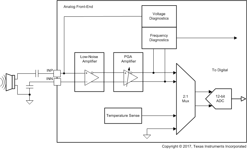
The analog front-end (AFE) in the PGA460-Q1 device, shown in #X1316, receives the reflected echo from the object, amplifies it, and feeds it into a digital signal processing (DSP) data path for echo detection. Because the received echo signal can vary amplitude (in millivolts for near objects and in microvolts for far objects), the first AFE stage is a very low-noise balanced amplifier with a predetermined fixed gain followed by a variable gain-stage amplifier with configurable gain from 32 dB to 90 dB. The amplified echo signal is converted into a digital signal by a 12-bit analog-to-digital converter (ADC) and fed to a DSP processing block for further evaluation and time-of-flight measurement.
The PGA460-Q1 AFE implements system diagnostics for sensing element (transducer) monitoring during the burst and decay stage of the echo recording process in a way of measuring the maximum achieved voltage at the transducer node and the frequency of oscillation at the transducer node. For more information on these diagnostics, see the GUID-BC9FDDC3-E4C4-4B97-827D-A2FCEED52928.html#TITLE-SLASEC8X133 section.
 Figure 7-3 Analog Front-End
The variable gain amplifier in the AFE implements a time-varying gain feature which allows the user to set different static gains and also specify a gain profile for the echo listening process (echo record time). This feature allows for a uniform amplification of echo signals from objects at different distances without saturating the ADC. As an example, for closer objects, gain can be programmed lower initially in time and then increased during the recording time to detect farther objects which have a very small echo signal. This feature helps in attaining sufficient SNR after ADC conversion for all distances for accurate time of flight measurement.
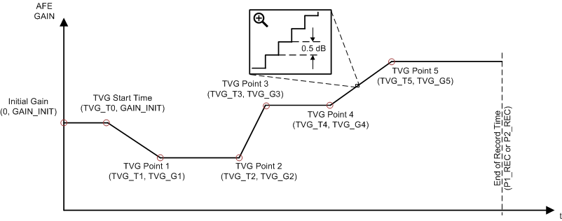
The time-varying gain parameters are stored in the EEPROM memory and characterized by:
- The initial fixed-gain parameter, GAIN_INIT.
- A time-varying gain start-time value stored in the TVGAIN0 register.
- An array of 5 gain-varying cross points placed in the TVGAIN0 to TVGAIN6 registers.
#X2707 shows an example plot of the time-varying gain.
 Figure 7-4 Time-Varying Gain Assignment Example
The time value, TVG start time, is expressed in terms of absolute time, and all following TVG point times (TVG_Tx parameters) are expressed as a delta time between the current and previous point. All gain values are expressed in an absolute gain value in dB and are unrelated from each other. The final gain setting of TVG Point 5 (TVG_G5) will be kept constant until the end of the echo record time. The time-varying gain assignment is the same for both presets. A linear interpolation scheme is used to calculate gain between two TVG points. The AFE gain resolution is 0.5 dB typical.
The time-varying gain changes during the recording are applied only on the record cycle that follows. If the TVGAIN[0:6] registers programmed to 0x00, the time-varying gain function of the PGA460-Q1 device is disabled and a fixed gain defined by the INIT_GAIN register is applied. In this case, changing the INIT_GAIN register changes the gain of AFE during the recording.
The offset on the time-varying gain is controlled through the two AFE_GAIN_RNG bits in DECPL_TEMP register. For each of the four settings as defined in the GUID-ED773D30-2D5D-4A9D-B0E9-278B351A9705.html#TITLE-SLASEC8X3442 section, the gain can be varied from 0 to 32 dB added on top of the offset.