SLVSDW2B December 2018 – November 2020 TPS23755
PRODUCTION DATA
- 1 Features
- 2 Applications
- 3 Description
- 4 Revision History
- 5 Pin Configuration and Functions
- 6 Specifications
-
7 Detailed Description
- 7.1 Overview
- 7.2 Functional Block Diagram
- 7.3
Feature Description
- 7.3.1 CLS Classification
- 7.3.2 DEN Detection and Enable
- 7.3.3 Internal Pass MOSFET
- 7.3.4
DC-DC Controller Features
- 7.3.4.1 VCC, VB and Advanced PWM Startup
- 7.3.4.2 CS, Current Slope Compensation and Blanking
- 7.3.4.3 COMP, FB, CP and Opto-less Feedback
- 7.3.4.4 FRS Frequency Setting and Synchronization
- 7.3.4.5 Frequency Dithering for Spread Spectrum Applications
- 7.3.4.6 SST and Soft-Start of the Switcher
- 7.3.4.7 AUX_V, AUX_D and Secondary Adapter Or'ing
- 7.3.5 Internal Switching FET - DRAIN, RSNS, SRF and SRR
- 7.3.6 VPD Supply Voltage
- 7.3.7 VDD Supply Voltage
- 7.3.8 GND
- 7.3.9 VSS
- 7.3.10 Exposed Thermal PAD
- 7.4 Device Functional Modes
-
8 Application and Implementation
- 8.1 Application Information
- 8.2
Typical Application
- 8.2.1 Design Requirements
- 8.2.2
Detailed Design Procedure
- 8.2.2.1 Input Bridges and Schottky Diodes
- 8.2.2.2 Protection, D1
- 8.2.2.3 Capacitor, C1
- 8.2.2.4 Detection Resistor, RDEN
- 8.2.2.5 Classification Resistor, RCLS
- 8.2.2.6 Bulk Capacitance, CBULK
- 8.2.2.7 Output Voltage Feedback Divider, RAUX, R1,R2
- 8.2.2.8 Setting Frequency, RFRS
- 8.2.2.9 Frequency Dithering, RDTR and CDTR
- 8.2.2.10 Bias Voltage, CVB and DVB
- 8.2.2.11 Transformer design, T1
- 8.2.2.12 Current Sense Resistor, RCS
- 8.2.2.13 Current Slope Compensation, RS
- 8.2.2.14 Bias Supply Requirements, CCC, DCC
- 8.2.2.15 Switching Transformer Considerations, RVCC and CCC2
- 8.2.2.16 Primary FET Clamping, RCL, CCL, and DCL
- 8.2.2.17 Converter Output Capacitance, COUT
- 8.2.2.18 Secondary Output Diode Rectifier, DOUT
- 8.2.2.19 Slew rate control, RSRF and RSRR
- 8.2.2.20 Shutdown at Low Temperatures, DVDD and CVDD
- 8.2.3 Application Curves
- 9 Power Supply Recommendations
- 10Layout
- 11Device and Documentation Support
- 12Mechanical, Packaging, and Orderable Information
Package Options
Mechanical Data (Package|Pins)
- RJJ|23
Thermal pad, mechanical data (Package|Pins)
Orderable Information
7.4.7 Start-Up and Converter Operation
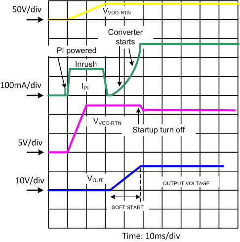
The internal PoE undervoltage lockout (UVLO) circuit holds the hotswap switch off before the PSE provides full voltage to the PD. This prevents the converter circuits from loading the PoE input during detection and classification. The converter circuits discharges CDD, CCC, and CVB while the PD is unpowered. Thus VVDD-RTN will be a small voltage until just after full voltage is applied to the PD, as seen in Figure 7-7.
The PSE drives the PD input voltage to the operating range once it has decided to power up the PD. When VPD rises above the UVLO turnon threshold (VUVLO-R, approximately 35.5 V) with RTN high, the TPS23755 enables the hotswap MOSFET with an approximately 140-mA (inrush) current limit. See the waveforms of Figure 7-8 for an example. Converter switching is disabled while CDD charges and VRTN falls from VVDD to nearly VVSS; however, the converter start-up circuit is allowed to charge CCC. Once the inrush current falls about 10% below the inrush current limit, the PD control switches to the operational level (approximately 450 mA) and converter switching is permitted.
Converter switching is allowed if the PD is not in inrush current limit and the VCC under-voltage lockout (VCUVR) circuit permits it. Continuing the start-up sequence shown in Figurer 7-7, VVCC rises as the start-up current source charges CCC and the converter switching is inhibited by the status of the VCC UVLO. The VB regulator powers the internal converter circuits as VVCC rises.
Once VVCC goes above its UVLO (nominally 8.25 V), the converter switching is enabled following the closed loop controlled soft-start sequence. Note that the startup current source capability is such that it can fully maintain VVCC during the converter soft-start without requiring any significant CCC capacitance, in 48 V input applications. At the end of the soft-start period, the startup current source is turned off. VVCC falls as it powers the internal circuits including the switching MOSFET gate. If the converter control-bias output rises to support VVCC before it falls to VCUVF (nominally 6.1 V), a successful start-up occurs. Figure 7-7 shows a small droop in VVCC while the output voltage rises smoothly and a successful start-up occurs.
 Figure 7-8 Power Up and Start
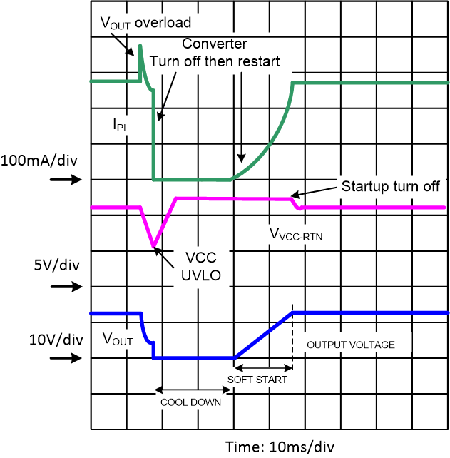
The converter shuts off when VVCC falls below its lower UVLO. This can happen when power is removed from the PD, or during a fault on a converter output rail. When one output is shorted, all the output voltages fall including the one that powers VCC. The control circuit discharges VCC until it hits the lower UVLO and turns off. A restart initiates if the converter turns off and there is sufficient VDD voltage. This type of operation is sometimes referred to as hiccup mode, which when combined with the soft-start provides robust output short protection by providing time-average heating reduction of the output rectifier.
Figure 7-9 illustrates the situation when there is severe overload at the main output which causes VCC hiccup. After VCC went below its UVLO due to the overload, the startup source is turned back on. Then, a new soft-start cycle is reinitiated, introducing a short pause before the output voltage is ramped up.
 Figure 7-9 Restart Following Severe Overload at Main Output of Flyback DC-DC Converter
If VVPD-VSS drops below the lower PoE UVLO (UVLO_R – UVLO_H, approximately 31 V), the hotswap MOSFET is turned off, but the converter still runs. The converter stops if VVCC falls below the VCUVF (nominally 6.1 V), the hotswap is in inrush current limit, the SST pin is pulled to ground, VVDD-RTN falls below typically 7.7 V (approximately 0.75 V hysteresis) or the converter is in thermal shutdown.