SLVSDW2B December 2018 – November 2020 TPS23755
PRODUCTION DATA
- 1 Features
- 2 Applications
- 3 Description
- 4 Revision History
- 5 Pin Configuration and Functions
- 6 Specifications
-
7 Detailed Description
- 7.1 Overview
- 7.2 Functional Block Diagram
- 7.3
Feature Description
- 7.3.1 CLS Classification
- 7.3.2 DEN Detection and Enable
- 7.3.3 Internal Pass MOSFET
- 7.3.4
DC-DC Controller Features
- 7.3.4.1 VCC, VB and Advanced PWM Startup
- 7.3.4.2 CS, Current Slope Compensation and Blanking
- 7.3.4.3 COMP, FB, CP and Opto-less Feedback
- 7.3.4.4 FRS Frequency Setting and Synchronization
- 7.3.4.5 Frequency Dithering for Spread Spectrum Applications
- 7.3.4.6 SST and Soft-Start of the Switcher
- 7.3.4.7 AUX_V, AUX_D and Secondary Adapter Or'ing
- 7.3.5 Internal Switching FET - DRAIN, RSNS, SRF and SRR
- 7.3.6 VPD Supply Voltage
- 7.3.7 VDD Supply Voltage
- 7.3.8 GND
- 7.3.9 VSS
- 7.3.10 Exposed Thermal PAD
- 7.4 Device Functional Modes
-
8 Application and Implementation
- 8.1 Application Information
- 8.2
Typical Application
- 8.2.1 Design Requirements
- 8.2.2
Detailed Design Procedure
- 8.2.2.1 Input Bridges and Schottky Diodes
- 8.2.2.2 Protection, D1
- 8.2.2.3 Capacitor, C1
- 8.2.2.4 Detection Resistor, RDEN
- 8.2.2.5 Classification Resistor, RCLS
- 8.2.2.6 Bulk Capacitance, CBULK
- 8.2.2.7 Output Voltage Feedback Divider, RAUX, R1,R2
- 8.2.2.8 Setting Frequency, RFRS
- 8.2.2.9 Frequency Dithering, RDTR and CDTR
- 8.2.2.10 Bias Voltage, CVB and DVB
- 8.2.2.11 Transformer design, T1
- 8.2.2.12 Current Sense Resistor, RCS
- 8.2.2.13 Current Slope Compensation, RS
- 8.2.2.14 Bias Supply Requirements, CCC, DCC
- 8.2.2.15 Switching Transformer Considerations, RVCC and CCC2
- 8.2.2.16 Primary FET Clamping, RCL, CCL, and DCL
- 8.2.2.17 Converter Output Capacitance, COUT
- 8.2.2.18 Secondary Output Diode Rectifier, DOUT
- 8.2.2.19 Slew rate control, RSRF and RSRR
- 8.2.2.20 Shutdown at Low Temperatures, DVDD and CVDD
- 8.2.3 Application Curves
- 9 Power Supply Recommendations
- 10Layout
- 11Device and Documentation Support
- 12Mechanical, Packaging, and Orderable Information
Package Options
Mechanical Data (Package|Pins)
- RJJ|23
Thermal pad, mechanical data (Package|Pins)
Orderable Information
7.4.8 PD Self-Protection
The PD section has the following self-protection functions.
- Hotswap switch current limit
- Hotswap switch foldback
- Hotswap thermal protection
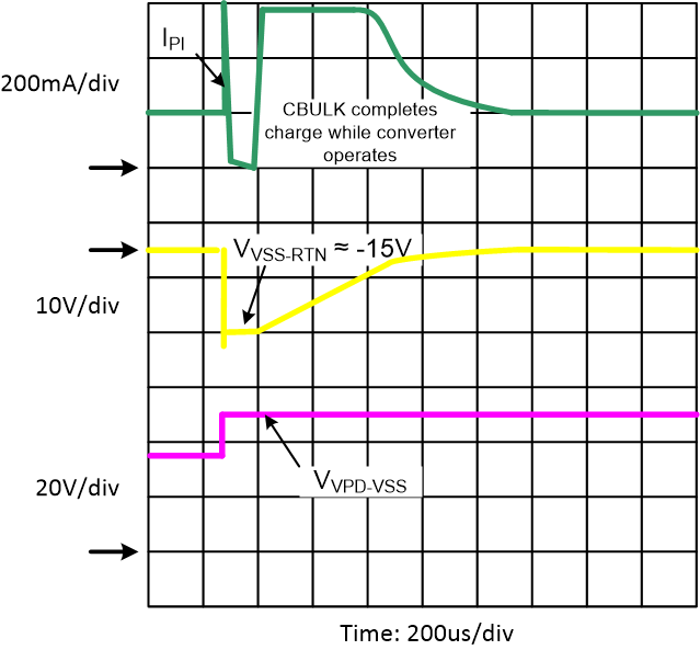
The internal hotswap MOSFET is protected against output faults with a current limit and deglitched foldback. The PSE output cannot be relied on to protect the PD MOSFET against transient conditions, requiring the PD to provide fault protection. High stress conditions include converter output shorts, shorts from VDD to RTN, or transients on the input line. An overload on the pass MOSFET engages the current limit, with VRTN-VSS rising as a result. If VRTN rises above approximately 12.3 V for longer than approximately 400 μs, the current limit reverts to the inrush limit, and turns the converter off. The 400-μs deglitch feature prevents momentary transients from causing a PD reset, provided that recovery lies within the bounds of the hotswap and PSE protection. Figure 7-10 shows an example of recovery from a 15-V PSE rising voltage step. The hotswap MOSFET goes into current limit, overshooting to a relatively low current, recovers to 420 mA, full-current limit, and charges the input capacitor while the converter continues to run. The MOSFET did not go into foldback because VRTN-VSS was below 12 V after the 400-μs deglitch.
 Figure 7-10 Response to PSE Step Voltage
The PD control has a thermal sensor that protects the internal hotswap MOSFET. Conditions like start-up or operation into a VPD to RTN short cause high power dissipation in the MOSFET. An overtemperature shutdown (OTSD) turns off the hotswap MOSFET and class regulator, which are restarted after the device cools. The PD restarts in inrush current limit when exiting from a PD overtemperature event.
Pulling DEN to VSS during powered operation causes the internal hotswap MOSFET to turn off. This feature allows a PD with secondary-side adapter ORing to achieve adapter priority. Take care with synchronous converter topologies that can deliver power in both directions.
The hotswap switch is forced off under the following conditions:
- VDEN ≤ VPD_DIS when VVPD-VSS is in the operational range
- PD over temperature
- VVPD-VSS < PoE UVLO (approximately 31 V)