SLVSDW2B December 2018 – November 2020 TPS23755
PRODUCTION DATA
- 1 Features
- 2 Applications
- 3 Description
- 4 Revision History
- 5 Pin Configuration and Functions
- 6 Specifications
-
7 Detailed Description
- 7.1 Overview
- 7.2 Functional Block Diagram
- 7.3
Feature Description
- 7.3.1 CLS Classification
- 7.3.2 DEN Detection and Enable
- 7.3.3 Internal Pass MOSFET
- 7.3.4
DC-DC Controller Features
- 7.3.4.1 VCC, VB and Advanced PWM Startup
- 7.3.4.2 CS, Current Slope Compensation and Blanking
- 7.3.4.3 COMP, FB, CP and Opto-less Feedback
- 7.3.4.4 FRS Frequency Setting and Synchronization
- 7.3.4.5 Frequency Dithering for Spread Spectrum Applications
- 7.3.4.6 SST and Soft-Start of the Switcher
- 7.3.4.7 AUX_V, AUX_D and Secondary Adapter Or'ing
- 7.3.5 Internal Switching FET - DRAIN, RSNS, SRF and SRR
- 7.3.6 VPD Supply Voltage
- 7.3.7 VDD Supply Voltage
- 7.3.8 GND
- 7.3.9 VSS
- 7.3.10 Exposed Thermal PAD
- 7.4 Device Functional Modes
-
8 Application and Implementation
- 8.1 Application Information
- 8.2
Typical Application
- 8.2.1 Design Requirements
- 8.2.2
Detailed Design Procedure
- 8.2.2.1 Input Bridges and Schottky Diodes
- 8.2.2.2 Protection, D1
- 8.2.2.3 Capacitor, C1
- 8.2.2.4 Detection Resistor, RDEN
- 8.2.2.5 Classification Resistor, RCLS
- 8.2.2.6 Bulk Capacitance, CBULK
- 8.2.2.7 Output Voltage Feedback Divider, RAUX, R1,R2
- 8.2.2.8 Setting Frequency, RFRS
- 8.2.2.9 Frequency Dithering, RDTR and CDTR
- 8.2.2.10 Bias Voltage, CVB and DVB
- 8.2.2.11 Transformer design, T1
- 8.2.2.12 Current Sense Resistor, RCS
- 8.2.2.13 Current Slope Compensation, RS
- 8.2.2.14 Bias Supply Requirements, CCC, DCC
- 8.2.2.15 Switching Transformer Considerations, RVCC and CCC2
- 8.2.2.16 Primary FET Clamping, RCL, CCL, and DCL
- 8.2.2.17 Converter Output Capacitance, COUT
- 8.2.2.18 Secondary Output Diode Rectifier, DOUT
- 8.2.2.19 Slew rate control, RSRF and RSRR
- 8.2.2.20 Shutdown at Low Temperatures, DVDD and CVDD
- 8.2.3 Application Curves
- 9 Power Supply Recommendations
- 10Layout
- 11Device and Documentation Support
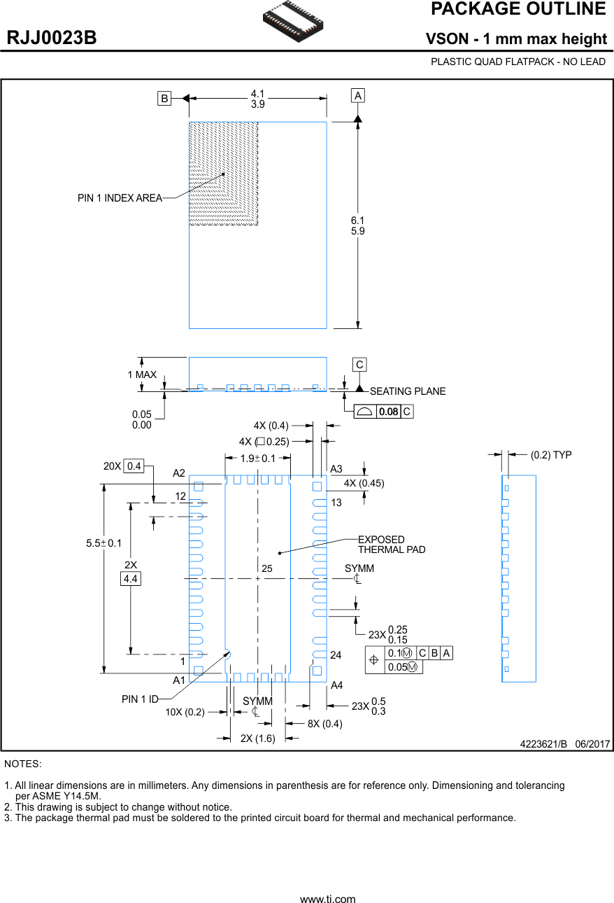
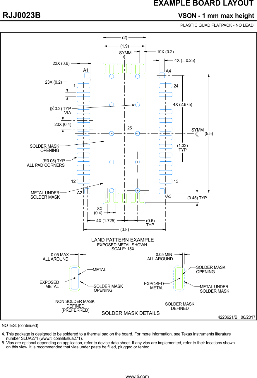
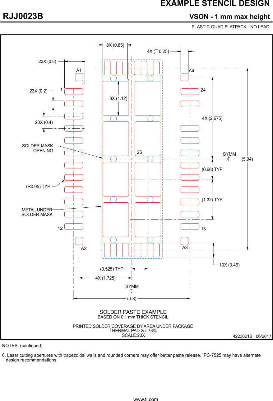
- 12Mechanical, Packaging, and Orderable Information
Package Options
Mechanical Data (Package|Pins)
- RJJ|23
Thermal pad, mechanical data (Package|Pins)
Orderable Information
12 Mechanical, Packaging, and Orderable Information
The following pages include mechanical, packaging, and orderable information. This information is the most current data available for the designated devices. This data is subject to change without notice and revision of this document. For browser-based versions of this data sheet, refer to the left-hand navigation.