SLVSDE4E march 2017 – june 2023 TPS61253A , TPS61253E
PRODUCTION DATA
- 1
- 1 Features
- 2 Applications
- 3 Description
- 4 Revision History
- 5 Device Comparison
- 6 Pin Configuration and Functions
- 7 Specifications
- 8 Detailed Description
- 9 Application and Implementation
- Power Supply Recommendations
- 10Layout
- 11Device and Documentation Support
- Mechanical, Packaging, and Orderable Information
Package Options
Mechanical Data (Package|Pins)
- YFF|9
Thermal pad, mechanical data (Package|Pins)
Orderable Information
9.2.2.3 Output Capacitor
For the output capacitor, it is recommended to use small ceramic capacitors placed as close as possible to the VOUT and GND pins of the IC. If, for any reason, the application requires the use of large capacitors which cannot be placed close to the IC, using a smaller ceramic capacitor in parallel to the large one is highly recommended. This small capacitor should be placed as close as possible to the VOUT and GND pins of the IC. To get an estimate of the recommended minimum output capacitance, Equation 6 can be used.
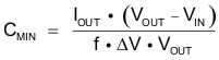
where
- f is the switching frequency which is 3.8 MHz (typ.)
- ΔV is the maximum allowed output ripple
With a chosen ripple voltage of 25 mV, a minimum effective capacitance of 7 μF is needed for maximum 1500-mA load. The capacitor can be smaller if the load is lower or the ripple can be larger. The total ripple is larger due to the ESR of the output capacitor. This additional component of the ripple can be calculated using Equation 7

An MLCC capacitor with twice the value of the calculated minimum should be used due to DC bias effects. This is required to maintain control loop stability. The output capacitor requires either an X7R or X5R dielectric. Y5V and Z5U dielectric capacitors, aside from their wide variation in capacitance over temperature, become resistive at high frequencies. There are no additional requirements regarding minimum ESR. Larger capacitors cause lower output voltage ripple as well as lower output voltage drop during load transients but the total effective output capacitance value should not exceed ca. 30 µF.
DC bias effect: high cap. ceramic capacitors exhibit DC bias effects, which have a strong influence on the effective capacitance of the device. Therefore, the right capacitor value has to be chosen very carefully. Package size and voltage rating in combination with material are responsible for differences between the rated capacitor value and effective capacitance. For instance, a 10-µF X5R 6.3-V 0603 MLCC capacitor would typically show an effective capacitance of less than 4 µF under 5 V bias condition.