SLVSDE4E march   2017  – june 2023 TPS61253A , TPS61253E

PRODUCTION DATA  

  1.   1
  2. Features
  3. Applications
  4. Description
  5. Revision History
  6. Device Comparison
  7. Pin Configuration and Functions
  8. Specifications
    1. 7.1 Absolute Maximum Ratings
    2. 7.2 ESD Ratings
    3. 7.3 Recommended Operating Conditions
    4. 7.4 Thermal Information
    5. 7.5 Electrical Characteristics
    6. 7.6 Timing Requirements
    7. 7.7 Switching Characteristics
    8. 7.8 Typical Characteristics
  9. Detailed Description
    1. 8.1 Overview
    2. 8.2 Functional Block Diagram
    3. 8.3 Feature Description
      1. 8.3.1 Start-up
      2. 8.3.2 Enable and Disable
      3. 8.3.3 Undervoltage Lockout (UVLO)
      4. 8.3.4 Current Limit Operation
      5. 8.3.5 Load Disconnection
      6. 8.3.6 Thermal Shutdown
    4. 8.4 Device Functional Modes
      1. 8.4.1 Auto PFM Mode
      2. 8.4.2 Forced PWM Mode
      3. 8.4.3 Ultrasonic Mode
      4. 8.4.4 Pass-Through Mode
  10. Application and Implementation
    1. 9.1 Application Information
    2. 9.2 Typical Application
      1. 9.2.1 Design Requirements
      2. 9.2.2 Detailed Design Procedure
        1. 9.2.2.1 Custom Design With WEBENCH® Tools
        2. 9.2.2.2 Inductor Selection
        3. 9.2.2.3 Output Capacitor
        4. 9.2.2.4 Input Capacitor
        5. 9.2.2.5 Checking Loop Stability
        6. 9.2.2.6 Application Curves
      3. 9.2.3 System Examples
  11.   Power Supply Recommendations
  12. 10Layout
    1. 10.1 Layout Guidelines
    2. 10.2 Layout Example
    3. 10.3 Thermal Considerations
  13. 11Device and Documentation Support
    1. 11.1 Device Support
      1. 11.1.1 Third-Party Products Disclaimer
      2. 11.1.2 Development Support
        1. 11.1.2.1 Custom Design With WEBENCH® Tools
    2. 11.2 Documentation Support
      1. 11.2.1 Related Documentation
    3. 11.3 Receiving Notification of Documentation Updates
    4. 11.4 Support Resources
    5. 11.5 Trademarks
    6. 11.6 Electrostatic Discharge Caution
    7. 11.7 Glossary
  14.   Mechanical, Packaging, and Orderable Information

Package Options

Mechanical Data (Package|Pins)
Thermal pad, mechanical data (Package|Pins)
Orderable Information

Application Curves

This section is based on the test results of TPS61253A, unless otherwise noted.
GUID-20201019-CA0I-KNCV-SZGT-LZX7LDGSQ5FM-low.gif
VIN = 3.6 V VOUT = 5 A L = 0.56 μH
COUT = 10 μF + 2x 4.7 μF Load = 10 mA Auto PFM
Figure 9-2 Steady 10 mA
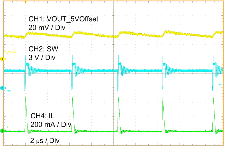
GUID-20201019-CA0I-TCMZ-ZNRK-P4NFFMBDMC3S-low.gif
VIN = 3.6 V VOUT = 5 A L = 0.56 μH
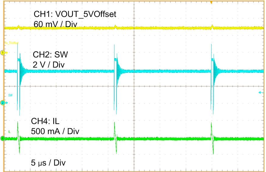
COUT = 10 μF + 2x 4.7 μF Load = 0 mA Auto PFM
Figure 9-4 Steady Ultrasonic Mode
GUID-20201019-CA0I-W8XC-TCNH-BGVQXMFN8RML-low.gif
VIN = 3.6 V VOUT = 5 A L = 0.56 μH
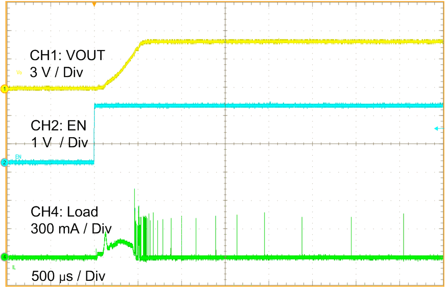
COUT = 10 μF + 2x 4.7 μF Load = 0 mA Auto PFM
Figure 9-6 Start-up by EN
GUID-20201019-CA0I-N4VD-KVXG-QKRGGR59X8NB-low.gif
VIN = 3.6 V VOUT = 5 V L = 0.56 μH
COUT = 10 μF Load = 0.5 A to 1 A, 20 μs/A Auto PFM
Figure 9-8 Load Transient with 10 μF COUT
GUID-20201019-CA0I-651D-9BKB-HSM29XH2S4Z7-low.gif
VIN = 3.6 V VOUT = 5 A L = 0.56 μH
COUT = 10 μF + 2x 4.7 μF Load = 1000 mA Auto PFM
Figure 9-3 Steady 1000 mA
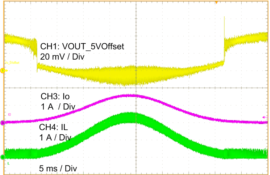
GUID-20201019-CA0I-3RPP-0BPP-CMQTFVQSDBGD-low.gif
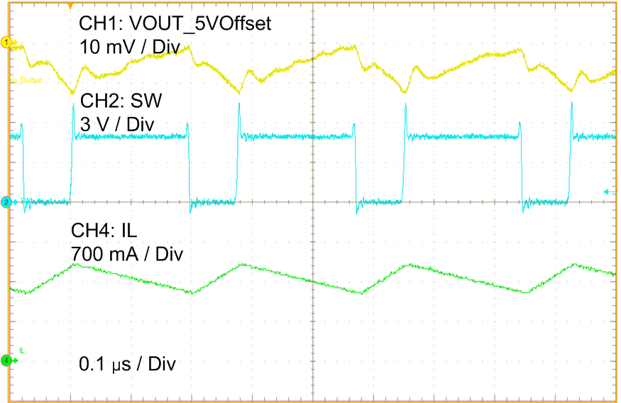
VIN = 3.6 V VOUT = 5 A L = 0.56 μH
COUT = 10 μF + 2x 4.7 μF Auto PFM
Figure 9-5 Load Sweep
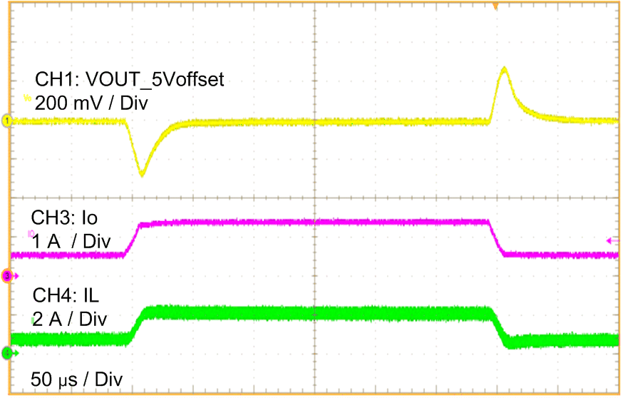
GUID-20201019-CA0I-0HS0-XBK7-XFL4RL9WDBTZ-low.gif
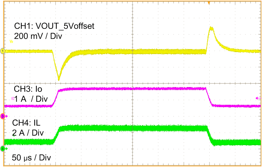
VIN = 3.6 V VOUT = 5 V L = 0.56 μH
COUT = 10 μF + 2x4.7 μF Load = 0.5 A to 1 A, 20 μs/A Auto PFM
Figure 9-7 Load Transient
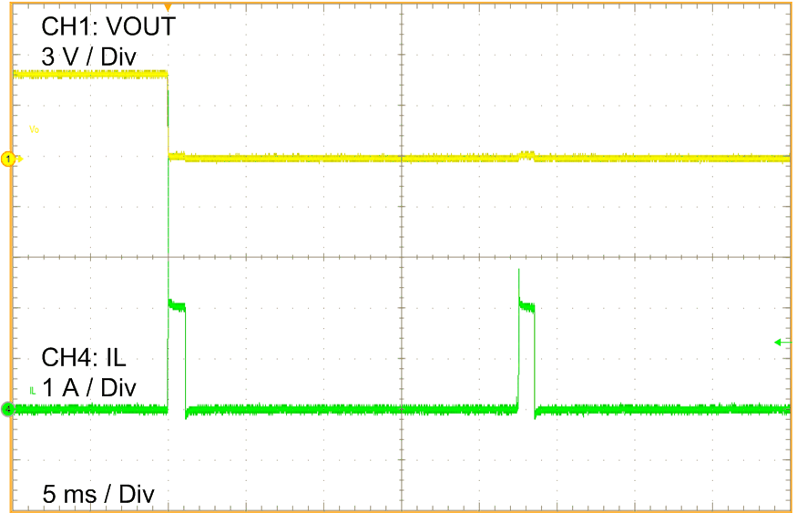
GUID-20201019-CA0I-TDXD-NPDD-4FQ75NRKSTX8-low.gif
VIN = 3.6 V VOUT = 5 V L = 0.56 μH
COUT = 10 μF + 2x4.7 μF Auto PFM
Figure 9-9 Short Output