JAJSQ88E february 2006 – october 2020 SN65LVDS301
PRODUCTION DATA
- 1
- 1 特長
- 2 アプリケーション
- 3 概要
- 4 Revision History
- 5 Pin Configuration and Functions
-
6 Specifications
- 6.1 Absolute Maximum Ratings #GUID-B6F760D2-14EB-4E2D-91AA-4EF9E63722A7/SLLS6819275
- 6.2 Thermal Information
- 6.3 Recommended Operating Conditions
- 6.4 Device Electrical Characteristics
- 6.5 Output Electrical Characteristics
- 6.6 Input Electrical Characteristics
- 6.7 Switching Characteristics
- 6.8 Timing Characteristics
- 6.9 Device Power Dissipation
- 6.10 Typical characteristics
- 7 Parameter Measurement Information
- 8 Detailed Description
- 9 Application information
- 10Power Supply Design Recommendation
- 11Layout
- 12Device and Documentation Support
- 13Mechanical, Packaging, and Orderable Information
5 Pin Configuration and Functions
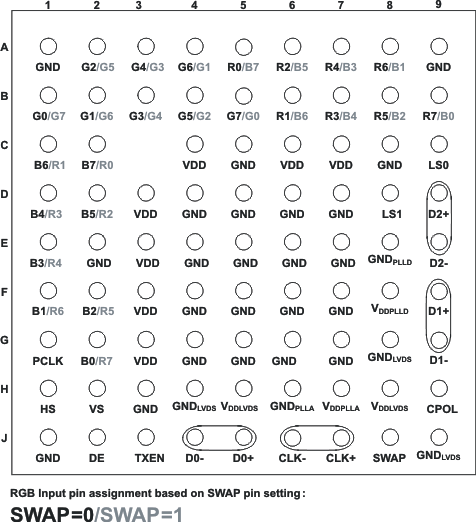
 Figure 5-1 80-Ball ZXH (Top View)
Pin Functions
| NAME | PIN | I/O | DESCRIPTION | |
|---|---|---|---|---|
| D0+, D0– | J5, J4 | SubLVDS Out | SubLVDS Data Link (active during normal operation) | |
| D1+, D1– | F9, G9 | SubLVDS Data Link (active during normal operation when LS0 = high and LS1 = low, or LS0 = low and LS1=high; high impedance if LS0 = LS1 = low) | ||
| D2+, D2– | D9, E9 | SubLVDS Data Link (active during normal operation when LS0 = low and LS1 = high, high-impedance when LS1 = low) | ||
| CLK+, CLK– | J7, J6 | SubLVDS output Clock; clock polarity is fixed | ||
| R0–R7 | A5/C2, B6/C1, A6/D2, B7/D1, A7/E1, B8/F2, A8/F1, B9/G2 | CMOS IN | Red Pixel Data (8); pin assignment depends on SWAP pin setting | |
| G0–G7 | B1/B5, B2/A4, A2/B4, B3/A3, A3/B3, B4/A2, A4/B2, B5/B1 | Green Pixel Data (8); pin assignment depends on SWAP pin setting | ||
| B0–B7 | B9/G2, A8/F1, B8/F2, A7/E1, B7/D1, A6/D2, B6/C1, A5/C2 | Blue Pixel Data (8); pin assignment depends on SWAP pin setting | ||
| HS | H1 | Horizontal Sync | ||
| VS | H2 | Vertical Sync | ||
| DE | J2 | Data Enable | ||
| PCLK | G1 | Input Pixel Clock; rising or falling clock polarity is selected by control input CPOL | ||
| LS0, LS1 | C9, D8 | Link Select (Determines active SubLVDS Data Links and PLL Range) See Table 8-2 | ||
| TXEN | J3 | Disables the CMOS Drivers and Turns Off the PLL, putting device in shutdown mode | ||
| 1 – Transmitter
enabled 0 – Transmitter disabled (Shutdown) |
||||
| Note: The TXEN input incorporates glitch-suppression logic to avoid device malfunction on short input spikes. It is necessary to pull TXEN high for longer than 10 μs to enable the transmitter. It is necessary to pull the TXEN input low for longer than 10 μs to disable the transmitter. At power up, the transmitter is enabled immediately if TXEN = 1 and disabled if TXEN = 0 | ||||
| CPOL | H9 | CMOS In | Input Clock Polarity Selection | |
| 0 – rising edge
clocking 1 – falling edge clocking |
||||
| SWAP | J8 | CMOS In | Bus Swap swaps the bus pins to allow device placement on top or bottom of pcb. See pinout drawing for pin assignments. | |
| 0 – data input
from B0...R7 1 – data input from R7...B0 |
||||
| VDD | C4 | Power Supply(1) | Supply Voltage | |
| GND | A1, A9, C5, C8, D4, D5, D6, D7, E2, E4, E5, E6, E7, F4, F5, F6, F7, G4, G5, G6, G7, H3, J1 | Supply Ground | ||
| VDDLVDS | H5, H8 | SubLVDS I/O supply Voltage | ||
| GNDLVDS | G8, H4 | SubLVDS Ground | ||
| VDDPLLA | H7 | PLL analog supply Voltage | ||
| GNDPLLA | H6 | PLL analog GND | ||
| VDDPLLD | F8 | PLL digital supply Voltage | ||
| GNDPLLD | E8 | PLL digital GND | ||
(1) For a multilayer pcb, it is recommended to keep one common GND layer
underneath the device and connect all ground terminals directly to this plane.