SLAA494B May 2011 – September 2023 MSP430AFE221 , MSP430AFE222 , MSP430AFE223 , MSP430AFE231 , MSP430AFE232 , MSP430AFE233 , MSP430AFE251 , MSP430AFE252 , MSP430AFE253
- 1
- Implementation of a Single-Phase Electronic Watt-Hour Meter Using the MSP430AFE2xx
- 1 Trademarks
- 2 Introduction
- 3 Block Diagram
- 4 Hardware Implementation
- 5 Software Implementation
- 6 Energy Meter Demo
- 7 Results
- 8 Important Notes
- 9 Schematics
- 10References
- 11Revision History
5.3.2 Phase Compensation
The CT, when used as a sensor, and the input circuit's passive components together introduce an additional phase shift between the current and voltage signals that needs compensation. The SD24 converter has built-in hardware delay that can be applied to individual samples when grouped. This delay can be used to provide the phase compensation required. This value is obtained during calibration and loaded on to the respective PRELOAD register for each converter. Figure 5-3 shows the application of PRELOAD.
 Figure 5-3 Phase Compensation Using PRELOAD Register
The fractional delay resolution is a function of input frequency (fin), OSR and the sampling frequency (fs).
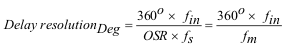
In this application for input frequency of 60 Hz, OSR of 256 and sampling frequency of 3906, the resolution for every bit in the preload register is approximately 0.02° with a maximum of 5.25° (maximum of 255 steps). Because the sampling of the three channels are group triggered, a method often used is to apply 128 steps of delay to all channels and then increase or decrease from this base value. This allows positive and negative delay timing to compensate for phase lead or lag. This puts the practical limit in the current design to ±2.62°. When using CTs that provide a larger phase shift than this maximum, an entire sample delay along with fractional delay must be provided. This phase compensation can also be modified on the fly to accommodate temperature drifts in CTs.