SNOA475F October 2016 – September 2020 LMV791
- Trademarks
- 1Introduction
-
2What Parameters Should Be Tested?
- 2.1 Open-Loop Gain (AOL) and Phase Margin
- 2.2 Slew Rate
- 2.3 Common-Mode Rejection Ratio (CMRR) and Power Supply Rejection Ratio (PSRR)
- 2.4 Open-Loop Output Impedance (Zo)
- 2.5 Voltage Noise (en)
- 2.6 Current Noise (in)
- 2.7 Input Offset Voltage (VOS), Input Bias Current (Ib), and Quiescent Current (IQ)
- 2.8 Output Voltage Versus Output Current (Claw Curve)
- 2.9 Overload Recovery Time (tOR)
- 2.10 Common-mode Input Capacitance (CCM) and Common-mode Differential Capacitance (CDIFF)
- 2.11 Overshoot and Transient Response
- 2.12 Common-Mode Voltage Range (CMVR)
- 3Conclusion
- Revision History
2.10 Common-mode Input Capacitance (CCM) and Common-mode Differential Capacitance (CDIFF)
There are two types of input capacitances, namely: a differential (CDIFF) and common-mode (CCM) . CDIFF, is the input capacitance between the non-inverting and inverting pins of an op amp. CCM, is the parasitic capacitance between each input pins and ground. Figure 2-34 shows a visual representation of CDIFF and CCM for OPA2375. Input capacitance can be found in the electrical characteristics table of the data sheet as shown in Figure 2-35.
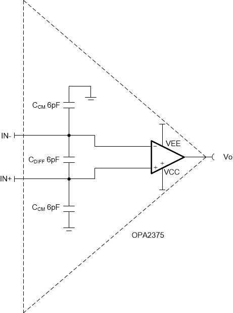 Figure 2-34 Input Capacitance Illustration
for OPA2375
 Figure 2-35 Data Sheet Specifications of
Input Capacitance Values for OPA2375
Figure 2-35 Data Sheet Specifications of
Input Capacitance Values for OPA2375with low input capacitance can help increase the frequency of pole in the feedback path far enough that it has negligible effect on the circuit. To ensure stability, it is important to make sure the pole created due to the interaction between input capacitance and the feedback impedance is at least 2 to 10 times larger in frequency as compared to the bandwidth of the circuit.
Figure 2-36 and Figure 2-38 show the circuits to simulate CCM and CDIFF. Ensure that the power supply voltage and other test conditions match closely with the op amp's datasheet. In the CCM test circuit, the op amp is configured as a buffer circuit with a 100kΩ in series with the non-inverting input of the op amp. Using the -3dB frequency of the bode plot at the non-inverting input of the op amp, CCM can be simulated and calculated as shown in Figure 2-37. Similarily Figure 2-39 shows the simulated CDIFF for OPA2375 and corresponding calculation. For more information on common-mode and differential input capacitances, please refer to "The Signal" authored by Bruce Trump. This circuit may be simulated by downloading the AN1516 Test Circuits in either TINA-TI™ or PSpice® for TI.
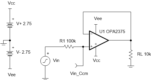 Figure 2-36 Common-Mode Input
Capacitance (CCM) Test Circuit
 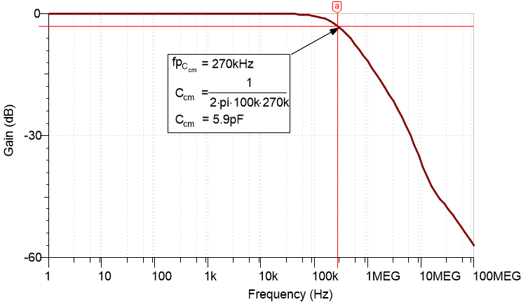 Figure 2-37 Simulated Common-Mode
Input Capacitance (CCM) for OPA2375
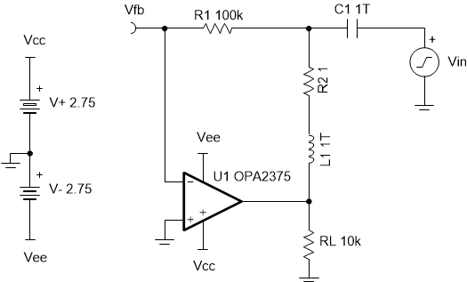 Figure 2-38 Differential Input
Capacitance (CDIFF) Test Circuit
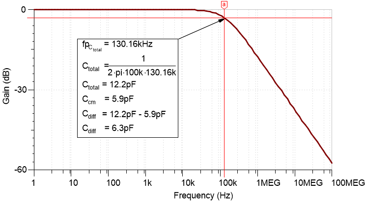 Figure 2-39 Simulated Differential
Input Capacitance (CDIFF) for OPA2375