SNOA475F October 2016 – September 2020 LMV791
- Trademarks
- 1Introduction
-
2What Parameters Should Be Tested?
- 2.1 Open-Loop Gain (AOL) and Phase Margin
- 2.2 Slew Rate
- 2.3 Common-Mode Rejection Ratio (CMRR) and Power Supply Rejection Ratio (PSRR)
- 2.4 Open-Loop Output Impedance (Zo)
- 2.5 Voltage Noise (en)
- 2.6 Current Noise (in)
- 2.7 Input Offset Voltage (VOS), Input Bias Current (Ib), and Quiescent Current (IQ)
- 2.8 Output Voltage Versus Output Current (Claw Curve)
- 2.9 Overload Recovery Time (tOR)
- 2.10 Common-mode Input Capacitance (CCM) and Common-mode Differential Capacitance (CDIFF)
- 2.11 Overshoot and Transient Response
- 2.12 Common-Mode Voltage Range (CMVR)
- 3Conclusion
- Revision History
2.8 Output Voltage Versus Output Current (Claw Curve)
Output voltage (Vout) versus output current (Iout) is usually referred to as the claw curve because they are shaped like an animal claw. Claw curves show the slam limit, or saturated output limit, with respect to output current and temperature. This is particularly important in rail to rail output amplifier models as it can help circuit designers to choose the appropriate op amp especially when driving heavy loads or when dynamic range is a concern. Figure 2-24 shows the data sheet claw curve for TLV9002. Claw curves are composed of two parts, the positive side (claw+) and the negative side (claw-). This value can be given in a data sheet as either absolute or relative. Absolute is when Vout is a specific power-supply voltage, whereas relative is when Vout is a generic power-supply voltage. To learn more about claw curves, please refer to the Texas Instruments Precision Labs video series on input and output limitations.
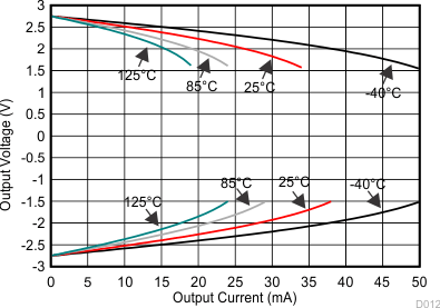 Figure 2-24 Data
sheet Graph Claw Curve for TLV9002
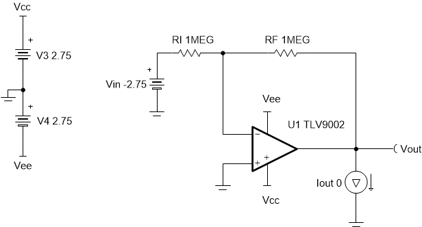 Figure 2-25 Claw+ Test
Circuit
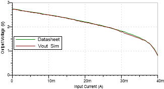 Figure 2-26 Simulated Claw+ Curve
(Sourcing) for TLV9002
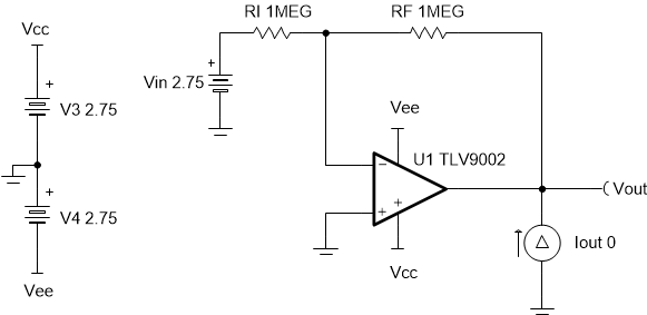 Figure 2-27 Claw- Test
Circuit
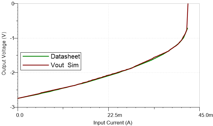 Figure 2-28 Simulated Claw- Curve
(Sinking) for TLV9002