SNOA475F October 2016 – September 2020 LMV791
- Trademarks
- 1Introduction
-
2What Parameters Should Be Tested?
- 2.1 Open-Loop Gain (AOL) and Phase Margin
- 2.2 Slew Rate
- 2.3 Common-Mode Rejection Ratio (CMRR) and Power Supply Rejection Ratio (PSRR)
- 2.4 Open-Loop Output Impedance (Zo)
- 2.5 Voltage Noise (en)
- 2.6 Current Noise (in)
- 2.7 Input Offset Voltage (VOS), Input Bias Current (Ib), and Quiescent Current (IQ)
- 2.8 Output Voltage Versus Output Current (Claw Curve)
- 2.9 Overload Recovery Time (tOR)
- 2.10 Common-mode Input Capacitance (CCM) and Common-mode Differential Capacitance (CDIFF)
- 2.11 Overshoot and Transient Response
- 2.12 Common-Mode Voltage Range (CMVR)
- 3Conclusion
- Revision History
2.9 Overload Recovery Time (tOR)
Driving the output beyond its linear range is called overloading the output. When the overload condition is corrected, there is a time delay before the overloaded output can recover. Overload recovery time (tOR) is the time required for the op amp to recover or catch-up to its rated output voltage from a saturated condition. This condition occurs when the amplifier is driven beyond its output swing limits causing the output to saturate. In other words tOR is the time required for all the internal transistors in the output stage to transition from an abnormal stage, whether saturated or cutoff, to a normal state. In some amplifiers, tOR increases for large input impedances. Usually, data sheet specification applies for low impedances and assumes that tOR is not degraded by stray capacitance. It is important to not exceed the absolute max limits when over-driving the device. To learn more about overload recovery time, please refer to the Texas Instruments Precision Labs video series on slew rate.
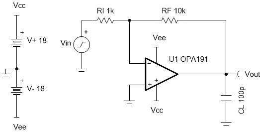
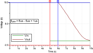
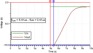
In addition to the input impedance, the tOR is also dependent on how strong the op amp is overdriven; the delay is much smaller when the op amp is barely overdriven as compared to significantly overdriven. There is overload recovery positive (tOR+) and overload recovery negative (tOR-), where tOR+ is referred to the positive supply and tOR- is referred to the negative supply. Figure 2-29 shows the data sheet overload recovery time for OPA191. Some data sheets only have one value for tOR, meaning it's the same delay for both positive and negative supply. Figure 2-30 and Figure 2-32 show the recommended circuit to simulate the positive and negative tOR respectively.
 Figure 2-29 Data Sheet
Specification of tOR for OPA191
Figure 2-29 Data Sheet
Specification of tOR for OPA191Figure 2-31 and Figure 2-33 show the simulated tOR+ and tOR- for OPA191. The simulated results below match well with the data sheet values, where tOR+ is equal to 0.4μs. The test circuit is a simple inverting amplifier with a gain of 10V/V. The input to this circuit is a piecewise function. Initially, the circuit outputs 18 V due to a DC level of -2V, after 5μs the output tries to catch up to the input. Notice here that the expected output is 20 V (DC level * Gain) but the output is limited to 18 V due to an output swing limitation, which is related to the supply rail. The time delay before the output reacts to the change in input is the tOR,. This circuit may be simulated by downloading the AN1516 Test Circuits in either TINA-TI™ or PSpice® for TI.
 Figure 2-30 Overload (Positive) Recovery Time Test
Circuit
 Figure 2-31 Simulated Overload (Positive) Recovery Time for
OPA191
 Figure 2-32 Overload (Negative) Recovery Time Test
Circuit
 Figure 2-33 Simulated Overload (Negative) Recovery Time for
OPA191