SNOA475F October 2016 – September 2020 LMV791
- Trademarks
- 1Introduction
-
2What Parameters Should Be Tested?
- 2.1 Open-Loop Gain (AOL) and Phase Margin
- 2.2 Slew Rate
- 2.3 Common-Mode Rejection Ratio (CMRR) and Power Supply Rejection Ratio (PSRR)
- 2.4 Open-Loop Output Impedance (Zo)
- 2.5 Voltage Noise (en)
- 2.6 Current Noise (in)
- 2.7 Input Offset Voltage (VOS), Input Bias Current (Ib), and Quiescent Current (IQ)
- 2.8 Output Voltage Versus Output Current (Claw Curve)
- 2.9 Overload Recovery Time (tOR)
- 2.10 Common-mode Input Capacitance (CCM) and Common-mode Differential Capacitance (CDIFF)
- 2.11 Overshoot and Transient Response
- 2.12 Common-Mode Voltage Range (CMVR)
- 3Conclusion
- Revision History
2.11 Overshoot and Transient Response
Transient response is an amplifiers response to a pulse input, and consists of large signal and small signal transient responses. Overshoot is important because it indicates how much ringing an amplifier has in the presence of a capacitive load. Overshoot is a measure of stability in time domain; it is the equivalent of what "peaking" is in the frequency domain. Some macro models use extra passive components to mimic the overshoot accurately but generally, if the phase margin is accurate, the overshoot should be accurate as well. Usually datasheets indicate whether a load capacitor was used when measuring the transient response, if so use the same capacitance value indicated in the data sheet. Figure 2-40 shows the test circuit for transient response (both small and large signal). This test circuit is simply a non-inverting amplifier with a gain of 1 V/V. The convention for small signal or large signal is dependent on the op amp and the process technology used. Typically, input signals less than 100 mV is considered small signal and input signal equal or greater than 1V is considered as a large signal. Figure 2-41 and Figure 2-42 show the small signal and large signal transient responses, respectively, for TLV9062.
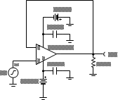 Figure 2-40 Transient Test
Circuit
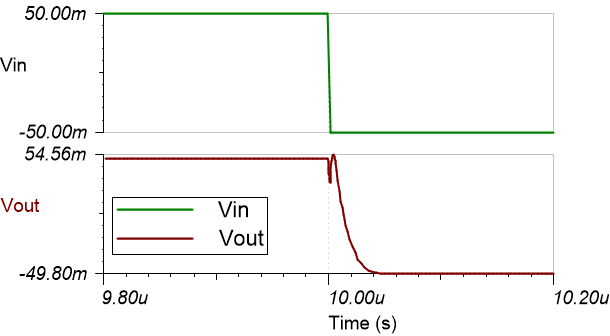 Figure 2-41 Small-Signal Transient Response for TLV9062
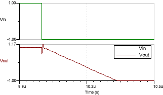 Figure 2-42 Large-Signal Transient Response for TLV9062
As you can see, the percent overshoot is much larger for small-signal as compared to large signal. Figure 2-43 shows the test circuit for overshoot and Figure 2-44 shows the corresponding simulation output of overshoot, which is confirmed in Figure 2-45. It's a simple inverting amplifier with a gain of 1V/V, with a resistive load of 10kΩ and capacitive load 100pF at the output. Capacitive loads at the output lowers the stability of an op amp circuit resulting in more overshoot as compared to a no-load circuit. This circuit may be simulated by downloading the AN1516 Test Circuits in either TINA-TI™ or PSpice® for TI.
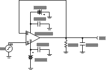 Figure 2-43 Overshoot Test
Circuit
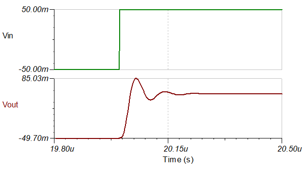 Figure 2-44 Simulated Overshoot Response for TLV9062
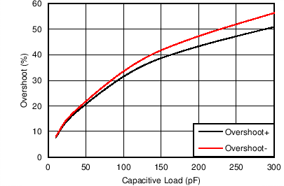 Figure 2-45 Data
Sheet Specification of Overshoot for TLV9062