SSZT430 August 2019 ISO5852S , LMG3410R070 , UCC21530 , UCC21710
As the number of electric vehicles (EVs) increase, there is a growing need to create more energy-efficient charging infrastructure systems around the world that can charge vehicles faster than ever before. New EVs have higher ranges and larger battery capacities than their predecessors, necessitating the development of fast DC charging solutions to support quick charging requirements. The DC charging station, according to Combined Charging System (CCS) and CHArge de MOve (CHAdeMO) standards, is a Level-3 charger that can deliver power between 120 kW and 240 kW. Today, it takes approximately 30 minutes for a 150-kW charging station to inject enough charge into an EV for it to travel about 250 km. Designing a single power processing unit to handle such a high amount of power requires complex multilevel topologies that are difficult to control.
In modern charging stations, one approach to scale the power output to the level required for fast charging is to use modular power converters stacked in parallel. Since the DC charging station will occupy significant volume and space, the power converters must be modular and optimized for high efficiency and high power density.
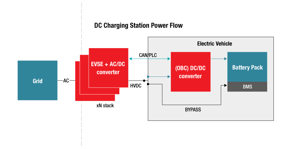
There are two paths to charge the battery pack. The first path is where the grid directly connects to the onboard charger (OBC) housed inside the vehicle. This OBC has AC/DC and DC/DC power conversion units that are typically rated up to 6.6 kW. In residential and commercial applications, these OBCs are capable of charging the battery in eight to 17 hours. The second path uses a separate physical charging station. Figure 1 shows the system architecture for a charging station. This path consists of a stack of AC/DC and DC/DC power processing units mounted outside the vehicle to interface the grid with the battery. These stacks of converters are directly connected to the battery, bypassing the OBC. Because these converters are not mounted inside the vehicle, they can be designed for high power levels, thereby enabling fast charging.
 Figure 1 DC Charging Station Architecture
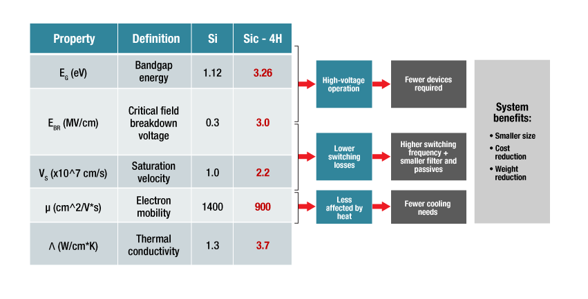
The first step toward increasing the power density is selecting the appropriate topology and components for the power stage. Wide bandgap devices like silicon carbide (SiC) offer the possibility of blocking very high DC link voltages compared to silicon insulated gate bipolar transistors (IGBTs). The converter can operate at a higher voltage, thus reducing the amount of current for the required power transfer. Reduced current directly translates to lesser copper usage, which increases the power density.
Transition to higher DC voltages also stresses the need for high-quality reinforced isolation. Our capacitive isolation technology, which includes gate drivers like the UCC21530, UCC21710 and ISO5852S, provides reinforced isolation up to 5.7 kVrms, making these devices suitable for SiC/IGBT applications. Figure 2 shows the benefits of using SiC.
 Figure 2 The Benefits of SiC for
Increasing Power Density in Charging Stations
Figure 2 The Benefits of SiC for
Increasing Power Density in Charging StationsSiC metal-oxide semiconductor field-effect transistors (MOSFETs) in the power stage help achieve high power density by moving to DC link voltages as high as 1,000 V/1,500 V. Using a multilevel topology to design high power converters is important, especially at 10 kW and beyond, because it reduces voltage stress on the devices and maintains acceptable levels of total harmonic distortion.
Our “Three-level, three-phase SiC AC-to-DC converter reference design” shows a T-type three-level converter where the switches in a T-type arm need to block only half the DC link voltage, thus enabling the selection of low-cost, low-voltage blocking devices driven by ISO5852S, which results in significant cost savings. A device like the LMG3410R070 could be used for the T-type branch of the inverter as well. Topology selection also plays a crucial role in the bidirectional operation of the converter, which is important for vehicle-to-grid applications.
The switching frequency has a direct impact on the size of magnetics and other passive components. There is a linear decrease in the size of the inductors and transformers when operated at high switching frequency. The use of SiC MOSFETs in the power stage enables operation at high switching frequencies, thereby improving the power density. SiC devices, with their superior on-state resistance and switching characteristics, also minimize the total losses, helping achieve high power density. An improvement in efficiency also means an improved thermal solution. Less heat dissipated across the components also improves the power density. Our C2000 real-time controllers are a perfect pairing for SiC MOSFETs, providing the performance and flexibility necessary for these high-frequency systems. Tools like Software Frequency Response Analyzer and Compensation Designer enable easy implementation of digital control algorithms.
Our high-quality components and system expertise can help you overcome fast EV charging challenges. The three-phase, three-level reference design as well as the “Bidirectional, dual active bridge reference design for level-3 electric vehicle charging stations” both operate as bidirectional converters with efficiencies greater than 97% and power densities around 1.4 kW/L (for the AC/DC stage) and 1.9 kW/L (for the DC/DC stage). These designs demonstrate using our gate drivers, real-time controllers and sensing technology to drive SiC MOSFETs of the power stage and also measure voltages and currents. They help meet the challenges of designing efficient, high-power-density, fast EV charging stations.