SLVA372D November 2009 – November 2022 LM2577 , LM2585 , LM2586 , LM2587 , LM2588 , LMR61428 , LMR62421 , LMR64010 , TL1451A , TL5001 , TL5001A , TLV61220 , TPS40210 , TPS40211 , TPS43000 , TPS61000 , TPS61002 , TPS61005 , TPS61006 , TPS61007 , TPS61010 , TPS61012 , TPS61013 , TPS61014 , TPS61015 , TPS61016 , TPS61020 , TPS61021A , TPS61024 , TPS61025 , TPS61026 , TPS61027 , TPS61028 , TPS61029 , TPS61029-Q1 , TPS61030 , TPS61031 , TPS61032 , TPS61046 , TPS61070 , TPS61071 , TPS61072 , TPS61073 , TPS61085 , TPS61086 , TPS61087 , TPS61088 , TPS61089 , TPS61090 , TPS61091 , TPS61092 , TPS61093 , TPS61093-Q1 , TPS61097-33 , TPS61100 , TPS61107 , TPS61120 , TPS61121 , TPS61122 , TPS61131 , TPS61170 , TPS61175 , TPS61175-Q1 , TPS61200 , TPS61201 , TPS61202 , TPS61220 , TPS61221 , TPS61222 , TPS61230A , TPS61235P , TPS61236P , TPS61240 , TPS61241 , TPS61253 , TPS61254 , TPS61256 , TPS61258 , TPS61259 , TPS612592 , TPS61291 , TPS65070 , TPS65072 , TPS65073 , TPS65100 , TPS65100-Q1 , TPS65101 , TPS65105 , TPS65130 , TPS65131 , TPS65131-Q1 , TPS65132 , TPS65132S , TPS65133 , TPS65137 , TPS65140 , TPS65140-Q1 , TPS65141 , TPS65142 , TPS65145 , TPS65145-Q1 , TPS65150 , TPS65150-Q1 , TPS65154 , TPS65155 , TPS65160 , TPS65160A , TPS65161 , TPS65161A , TPS65161B , TPS65162 , TPS65163 , TPS65167A , TPS65170 , TPS65175 , TPS65175B , TPS65175C , TPS65176 , TPS65177 , TPS65177A , TPS65178 , TPS65631 , TPS65631W , TPS65632 , TPS65632A , TPS65640 , TPS65642 , TPS65642A , UCC39411
- Basic Calculation of a Boost Converter's Power Stage
- 1 Basic Configuration of a Boost Converter
- 2 Calculate the Maximum Switch Current
- 3 Inductor Selection
- 4 Rectifier Diode Selection
- 5 Output Voltage Setting
- 6 Input Capacitor Selection
- 7 Output Capacitor Selection
- 8 Equations to Calculate the Power Stage of a Boost Converter
- 9 References
- 10Revision History
2 Calculate the Maximum Switch Current
The first step to calculate the switch current is to determine the duty cycle, D, for the minimum input voltage. The minimum input voltage is used because this leads to the maximum switch current.
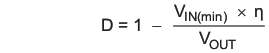
VIN(min) = minimum input
voltage
VOUT = desired output
voltage
η = efficiency of the converter, e.g.
estimated 80%
The efficiency is added to the duty cycle calculation, because the converter has to deliver also the energy dissipated. This calculation gives a more realistic duty cycle than just the equation without the efficiency factor.
Either an estimated factor, e.g. 80%
(which is not unrealistic for a boost converter worst case efficiency), can be used
or see the Typical Characteristics section of the selected converter's data
sheet
(Reference 3 and 4).
The next step to calculate the maximum switch current is to determine the inductor ripple current. In the converters data sheet normally a specific inductor or a range of inductors is named to use with the IC. So either use the recommended inductor value to calculate the ripple current, an inductor value in the middle of the recommended range or, if none is given in the data sheet, the one calculated in the Inductor Selection section of this application note.
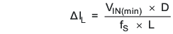
VIN(min) = minimum input
voltage
D = duty cycle calculated in Equation 1
fS = minimum switching frequency of
the converter
L = selected inductor value
Now it has to be determined if the selected IC can deliver the maximum output current.
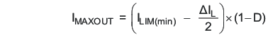
ILIM(min) = minimum value
of the current limit of the integrated switch (given in the data sheet)
ΔIL = inductor ripple current calculated
in Equation 2
D = duty cycle calculated in Equation 1
If the calculated value for the maximum output current of the selected IC, IMAXOUT, is below the systems required maximum output current, another IC with a higher switch current limit has to be used.
Only if the calculate value for IMAXOUT is just a little smaller than the needed one, it is possible to use the selected IC with an inductor with higher inductance if it is still in the recommended range. A higher inductance reduces the ripple current and therefore increases the maximum output current with the selected IC.
If the calculated value is above the maximum output current of the application, the maximum switch current in the system is calculated:
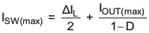
ΔIL = inductor ripple
current calculated in Equation 2
IOUT(max) = maximum output current
necessary in the application
D = duty cycle calculated
in Equation 1
This is the peak current, the inductor, the integrated switch(es) and the external diode has to withstand.