SPRUIR8B april 2020 – july 2023
- 1
- CLB Tool
- Trademarks
- 1Introduction
- 2Getting Started
- 3Using the CLB Tool
-
4Examples
- 4.1
Foundational Examples
- 4.1.1 CLB Empty Project
- 4.1.2 Example 3 – PWM Generation
- 4.1.3 Example 7 – State Machine
- 4.1.4 Example 13 – PUSH-PULL Interface
- 4.1.5 Example 14 – Multi-Tile
- 4.1.6 Example 15 – Tile to Tile Delay
- 4.1.7 Example 16 - Glue Logic
- 4.1.8 Exampe 18 - AOC
- 4.1.9 Example 19 - AOC Release Control
- 4.1.10 Example 20 - CLB XBARs
- 4.2
Getting Started Examples
- 4.2.1 Example 1 – Combinatorial Logic
- 4.2.2 Example 2 – GPIO Input Filter
- 4.2.3 Example 4 – PWM Protection
- 4.2.4 Example 5 – Event Window
- 4.2.5 Example 6 – Signal Generation and Check
- 4.2.6 Example 8 – External AND Gate
- 4.2.7 Example 9 – Timer
- 4.2.8 Example 10 – Timer With Two States
- 4.2.9 Example 11 – Interrupt Tag
- 4.2.10 Example 12 – Output Intersect
- 4.2.11 Example 17 – One-Shot PWM Generation
- 4.2.12 Example 21 - Clock Prescaler and NMI
- 4.2.13 Example 22 - Serializer
- 4.2.14 Example 23 - LFSR
- 4.2.15 Example 24 - Lock Output Mask
- 4.2.16 Example 25 - Input Pipeline Mode
- 4.2.17 Example 26 - Clocking Pipeline Mode
- 4.3 Expert Examples
- 4.1
Foundational Examples
- 5Enabling CLB Tool in Existing DriverLib Projects
- 6Frequently Asked Questions (FAQs)
- 7Revision History
4.2.1 Example 1 – Combinatorial Logic
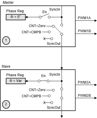
The objective of this example is to prevent simultaneous high or low outputs on a PWM pair. PWM modules 1 and 2 are configured to generate identical waveforms based on a fixed frequency up-count mode. The time-base of PWM2 is synchronized to that of PWM1 as shown in Figure 4-2.
 Figure 4-2 Example 1: EPWM
Synchronization
Figure 4-2 Example 1: EPWM
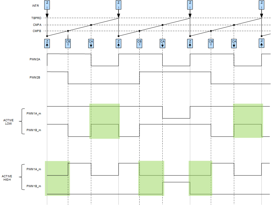
SynchronizationThe PWM waveforms are generated to deliberately force both outputs in each module to be simultaneously high and low at different times, as shown in Figure 4-3.
 Figure 4-3 Example 1: PWM Test
Pattern
Figure 4-3 Example 1: PWM Test
PatternThe intention is to modify these waveforms with the CLB to remove either simultaneous high or simultaneous low conditions. This represents a simple combinatorial logic example. The logic operates in three modes: normal, active high, and active low. In normal mode, the PWM signals are passed through the CLB un-modified. In active high mode, the logic prevents logical ‘1’ outputs from simultaneously appearing at the PWM pins. Similarly, in active low mode, logical ‘0’ outputs must not appear on both PWM pins. For instance, if the logic is in active low mode and both PWM signals are low, the output for both PWMs will be forced high. Refer to Table 4-2 for more details. The mode is selected using a 2-bit field as shown in Table 4-1.
| Mode Name | Type | [MODE 1] | [MODE 0] |
|---|---|---|---|
| M0 | Normal | 0 | 0 |
| M1 | Active Low | 0 | 1 |
| M2 | Active High | 1 | 0 |
| M3 | Reserved | 1 | 1 |
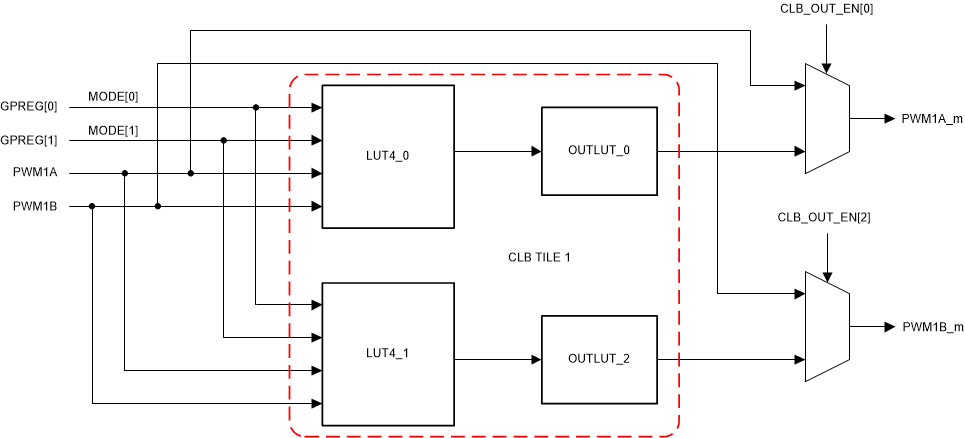
The logic circuit which implements the patterns is shown in Figure 4-4. Output signals have “_m” appended to the name to indicate they may have been modified by the CLB.
 Figure 4-4 Example 1: Logic
Diagram
Figure 4-4 Example 1: Logic
DiagramThe logic above can be implemented using two 4-input LUTs: one for each output signal. Therefore, only a small part of one CLB tile is involved. In the example, only the signals from the PWM1 module are modified by the CLB. The signals from PWM2 are carried directly to the device pins for comparison purposes. The input and output waveforms for PWM1 are shown in Figure 4-5 (modes 1 and 2). This image highlights in green the areas where the output is forced high or low by the CLB logic.
 Figure 4-5 Example 1: Generated
PWM
Figure 4-5 Example 1: Generated
PWM| Operating Mode | Original PWM A Output | Original PWM B Output | PWM A Output | PWM B Output |
|---|---|---|---|---|
| Normal | 0 | 0 | 0 | 0 |
| 0 | 1 | 0 | 1 | |
| 1 | 0 | 1 | 0 | |
| 1 | 1 | 1 | 1 | |
| Active Low | 0 | 0 | 1 | 1 |
| 0 | 1 | 0 | 1 | |
| 1 | 0 | 1 | 0 | |
| 1 | 1 | 1 | 1 | |
| Active High | 0 | 0 | 0 | 0 |
| 0 | 1 | 0 | 1 | |
| 1 | 0 | 1 | 0 | |
| 1 | 1 | 0 | 0 |
The required logic is implemented using 4-input LUTs 0 and 1. Each of these is connected to the two PWM signals, and the two LSBs of the software “mode” variable, which are written to the GPREG register. The CLB outputs are connected to the PWM1A and PWM1B signals which then go to GPIO pins and 1, respectively. Figure 4-6 conceptually shows the connections to and from the CLB tile.
 Figure 4-6 Example 1: CLB
Configuration
Figure 4-6 Example 1: CLB
ConfigurationTo run the example, follow this procedure:
- Click “Project → Import CCS Projects…”.
- Navigate to the CLB tool example directory. The path is:
- [C2000Ware]\driverlib\f2837xd\examples\cpu1\clb\ccs, or
- [C2000Ware]\driverlib\f28004x\examples\clb\ccs, or
- [C2000Ware]\driverlib\f2838x\examples\c28x\clb\ccs
In the description that follows, it is assumed the C2000Ware directory above is in use.
- Select the project “clb_ex1_combinatorial_logic” and click “Finish”.
- In the CCS Project Explorer window, expand the project “clb_ex1_combinatorial_logic” and open the file “clb_ex1_combinatorial_logic.syscfg”.
- Inspect the configuration of the tile and observe the logical expressions in LUT4_0 and LUT4_1, and the configuration of the output LUTs.
- From the CCS menu, select “Project → Build Project”.
- Monitor the pins.
- The Launchpad pins to watch the PWMs for the F28379D and Experimenter kit pins for F28388D are listed, but the Launchpad pins for other devices are not listed. Refer to the device datasheet for more information on available pins and their configurations
- Open a CCS Expressions window.
- [Optional] – for instructions on how to run a simulation of the CLB, see Section 3.5.3.
If running the program on an F28379D LaunchPad board, PWM signals 1A and 1B can be monitored on pins J4/40 and J4/39, respectively. Set up an oscilloscope to monitor the signals at these pins while the program is running.
If running the program on an experimenter’s kit fitted with a F28388D controlCARD, the signals can be found on pins 49 and 51, respectively.
Open a CCS Expressions window and add the program variable “mode”. With mode set to the default value of 0, the PWM signals pass through the CLB without modification. Stop the program and change mode to 1, then restart the program. The signals should be as shown in the timing diagram above. Repeat this procedure to change the mode to 2 and verify the signals are as shown in the previous timing diagram.