SPRUIR8B april 2020 – july 2023
- 1
- CLB Tool
- Trademarks
- 1Introduction
- 2Getting Started
- 3Using the CLB Tool
-
4Examples
- 4.1
Foundational Examples
- 4.1.1 CLB Empty Project
- 4.1.2 Example 3 – PWM Generation
- 4.1.3 Example 7 – State Machine
- 4.1.4 Example 13 – PUSH-PULL Interface
- 4.1.5 Example 14 – Multi-Tile
- 4.1.6 Example 15 – Tile to Tile Delay
- 4.1.7 Example 16 - Glue Logic
- 4.1.8 Exampe 18 - AOC
- 4.1.9 Example 19 - AOC Release Control
- 4.1.10 Example 20 - CLB XBARs
- 4.2
Getting Started Examples
- 4.2.1 Example 1 – Combinatorial Logic
- 4.2.2 Example 2 – GPIO Input Filter
- 4.2.3 Example 4 – PWM Protection
- 4.2.4 Example 5 – Event Window
- 4.2.5 Example 6 – Signal Generation and Check
- 4.2.6 Example 8 – External AND Gate
- 4.2.7 Example 9 – Timer
- 4.2.8 Example 10 – Timer With Two States
- 4.2.9 Example 11 – Interrupt Tag
- 4.2.10 Example 12 – Output Intersect
- 4.2.11 Example 17 – One-Shot PWM Generation
- 4.2.12 Example 21 - Clock Prescaler and NMI
- 4.2.13 Example 22 - Serializer
- 4.2.14 Example 23 - LFSR
- 4.2.15 Example 24 - Lock Output Mask
- 4.2.16 Example 25 - Input Pipeline Mode
- 4.2.17 Example 26 - Clocking Pipeline Mode
- 4.3 Expert Examples
- 4.1
Foundational Examples
- 5Enabling CLB Tool in Existing DriverLib Projects
- 6Frequently Asked Questions (FAQs)
- 7Revision History
4.2.2 Example 2 – GPIO Input Filter
This example demonstrates use of finite state machines (FSMs) and counters to implement a simple ‘glitch’ filter which might, for example, be applied to an incoming GPIO signal to remove unwanted short duration pulses.
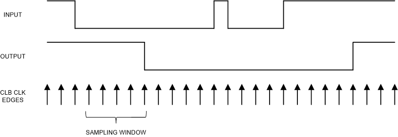
Figure 4-7 shows in principle what the glitch filter does. An incoming digital signal is sampled at the CLB clock rate and a counter counts the number of consecutive samples where the input is either high or low. If this number is equal to or greater than a specified sample window, the filter output takes on the same value as the input; otherwise the filter output does not change. Figure 4-7 shows in principle what the filter does.
 Figure 4-7 Example 2: GPIO Glitch
Example
Figure 4-7 Example 2: GPIO Glitch
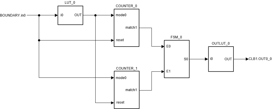
ExampleThe CLB configuration uses one LUT4 to invert the incoming signal, and two counters to count the number of pulses: one counter for the high pulses, the other for low pulses. When either counter reaches the sample window length a pulse appears at its ‘match1’ output. In this example the filter sample window length is set to eight. An FSM latches the pulse and implements a simple logic equation to determine the required level at its ‘S0’ state output. One output LUT is used to convey the FWM output to the peripheral signal multiplexer for connection to GPIO0. The CLB configuration is shown in Figure 4-8.
 Figure 4-8 Example 2: CLB
Configuration
Figure 4-8 Example 2: CLB
ConfigurationThe example code configures the ePWM1 module to generate the test stimulus.
To run the example, follow this procedure:
- In CCS v9.0 or higher, click “Project → Import CCS Projects…”.
- Navigate to the CLB tool example
directory. The path is:
- [C2000Ware]\driverlib\f2837xd\examples\cpu1\clb\ccs, or
- [C2000Ware]\driverlib\f28004x\examples\clb\ccs, or
- [C2000Ware]\driverlib\f2838x\examples\c28x\clb\ccs
In the description that follows, it is assumed the C2000Ware directory above is in use.
- Select the project “glitch_filter” and click “Finish”.
- In the CCS Project Explorer window, expand the project “glitch_filter” and open the file “tile.syscfg”.
- Inspect the configuration of the tile and observe the settings of the sub-modules LUT4_0, COUNTER_0, COUNTER_1, and FSM_0. Verify that the configuration matches that in the example description above.
- From the CCS menu, select “Project → Build Project”.
- [Optional] – for instructions on how to run a simulation of the CLB, see Section 3.5.3.
If running the program on an F28379D LaunchPad board, PWM signals 1A and 1B can be monitored on pins J4/40 and J4/39, respectively. Set up an oscilloscope to monitor the signals at these pins while the program is running. If running the program on an experimenter’s kit fitted with a F280049 or F28388D controlCARD, the signals can be found on pins 49 and 51, respectively.
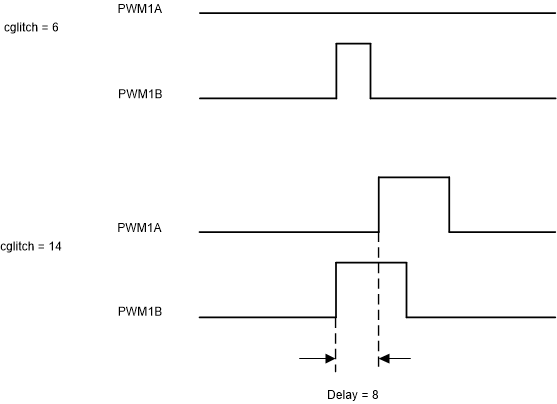
Open a CCS Expressions window and add the program variable “cglitch”. Run the program while observing PWM signals 1A and 1B. Pause the program and change the value of “cglitch”, then re-start the program (this process is easier if the expressions window is set to run in “continuous refresh”). For values of 7 or less the glitch should be removed by the filter because its’ width is less than the sample window. When “cglitch” is higher than 7 the glitch should appear on both outputs. Notice also that edges on PWM1A have a small delay compared with those on PWM1B. This is a consequence of the filter method used.
Figure 4-9 shows the expected waveforms at the output pins for glitch widths below and above the sample window setting of 8.
 Figure 4-9 Example 2: GPIO Glitch
Width