SBAS603B April 2013 – November 2020 ADS4449
PRODUCTION DATA
- 1 Features
- 2 Applications
- 3 Description
- 4 Revision History
- 5 Pin Configuration and Functions
- 6 Specifications
- 7 Parameter Measurement Information
-
8 Detailed Description
- 8.1 Overview
- 8.2 Functional Block Diagram
- 8.3 Feature Description
- 8.4 Device Functional Modes
- 8.5 Programming
- 8.6
Register Maps
- 8.6.1
Register Description
- 8.6.1.1 Register Address 00h (Default = 00h)
- 8.6.1.2 Register Address 01h (Default = 00h)
- 8.6.1.3 Register Address 25h (Default = 00h)
- 8.6.1.4 Register Address 2bh (Default = 00h)
- 8.6.1.5 Register Address 31h (Default = 00h)
- 8.6.1.6 Register Address 37h (Default = 00h)
- 8.6.1.7 Register Address 3dh (Default = 00h)
- 8.6.1.8 Register Address 3fh (Default = 00h)
- 8.6.1.9 Register Address 40h (Default = 00h)
- 8.6.1.10 Register Address 42h (Default = 00h)
- 8.6.1.11 Register Address 45h (Default = 00h)
- 8.6.1.12 Register Address 4ah (Defalut = 00h)
- 8.6.1.13 Register Address 62h (Default = 00h)
- 8.6.1.14 Register Address 7ah (Default = 00h)
- 8.6.1.15 Register Address 92h (Default = 00h)
- 8.6.1.16 Register Address A9h (Default = 00h)
- 8.6.1.17 Register Address Ach (Default = 00h)
- 8.6.1.18 Register Address C3h (Default = 00h)
- 8.6.1.19 Register Address C4h (Default = 00h)
- 8.6.1.20 Register Address Cfh (Default = 00h)
- 8.6.1.21 Register Address D6h (Default = 00h)
- 8.6.1.22 Register Address D7h (Default = 00h)
- 8.6.1.23 Register Address F1h (Default = 00h)
- 8.6.1.24 Register Address 58h (Default = 00h)
- 8.6.1.25 Register Address 59h (Default = 00h)
- 8.6.1.26 Register Address 70h (Default = 00h)
- 8.6.1.27 Register Address 71h (Default = 00h)
- 8.6.1.28 Register Address 88h (Default = 00h)
- 8.6.1.29 Register Address 89h (Default = 00h)
- 8.6.1.30 Register Address A0h (Default = 00h)
- 8.6.1.31 Register Address A1h (Default = 00h)
- 8.6.1.32 Register Address Feh (Default = 00h)
- 8.6.1
Register Description
- 9 Application and Implementation
- 10Power Supply Recommendations
- 11Layout
- 12Device and Documentation Support
Package Options
Mechanical Data (Package|Pins)
- ZCR|144
Thermal pad, mechanical data (Package|Pins)
Orderable Information
8.4.3 Using High SNR Mode Register Settings
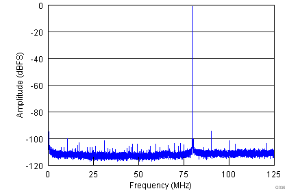
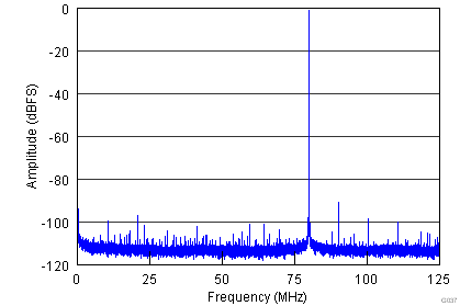
The HIGH SNR MODE register settings can be used to further improve the SNR. However, there is a trade off between improved SNR and degraded THD when these settings are used. These settings shut down the internal spectrum-cleaning algorithm, resulting in THD performance degradation. Figure 8-6 and Figure 8-7 show the effect of using HIGH SNR MODE. SNR improves by approximately 1 dB and THD degrades by 3 dB.

| fIN = 170 MHz | SFDR = 93 dBc | SNR = 69.1 dBFS |
| SINAD = 69 dBFS | THD = 89 dBc | |

| fIN = 170 MHz | SFDR = 89 dBc | SNR = 70.1 dBFS |
| SINAD = 70 dBFS | THD = 86 dBc | |
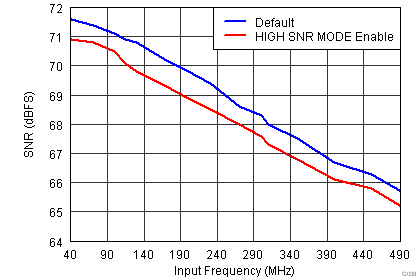
Figure 8-8 shows SNR versus input frequency with and without these settings.
 Figure 8-8 SNR vs Input Frequency with High SNR Mode
To obtain best performance, TI recommends keeping termination impedance between INP and INM low (for instance, at 50 Ω differential). This setting helps absorb the kickback noise component of the spectrum-cleaning algorithm. However, when higher termination impedances (such as 100 Ω) are required, shutting down the spectrum-cleaning algorithm by using the HIGH SNR MODE register settings can be helpful.