SLAS708A September 2010 – September 2019 ADS7947 , ADS7948 , ADS7949
PRODUCTION DATA.
- 1 Features
- 2 Applications
- 3 Description
- 4 Revision History
- 5 Device Comparison Table
- 6 Pin Configuration and Functions
-
7 Specifications
- 7.1 Absolute Maximum Ratings
- 7.2 ESD Ratings
- 7.3 Recommended Operating Conditions: ADS794x (12-, 10-, 8-Bit)
- 7.4 Thermal Information
- 7.5 Electrical Characteristics: ADS7947 (12-Bit)
- 7.6 Electrical Characteristics: ADS7948 (10-Bit)
- 7.7 Electrical Characteristics: ADS7949 (8-Bit)
- 7.8 Timing Requirements
- 7.9 Switching Characteristics
- 7.10 Typical Characteristics: ADS7947, ADS7948, ADS7949
- 7.11 Typical Characteristics: ADS7947 (12-Bit)
- 8 Detailed Description
- 9 Application and Implementation
- 10Power Supply Recommendations
- 11Layout
- 12Device and Documentation Support
- 13Mechanical, Packaging, and Orderable Information
Package Options
Mechanical Data (Package|Pins)
- RTE|16
Thermal pad, mechanical data (Package|Pins)
- RTE|16
Orderable Information
11.2 Layout Example
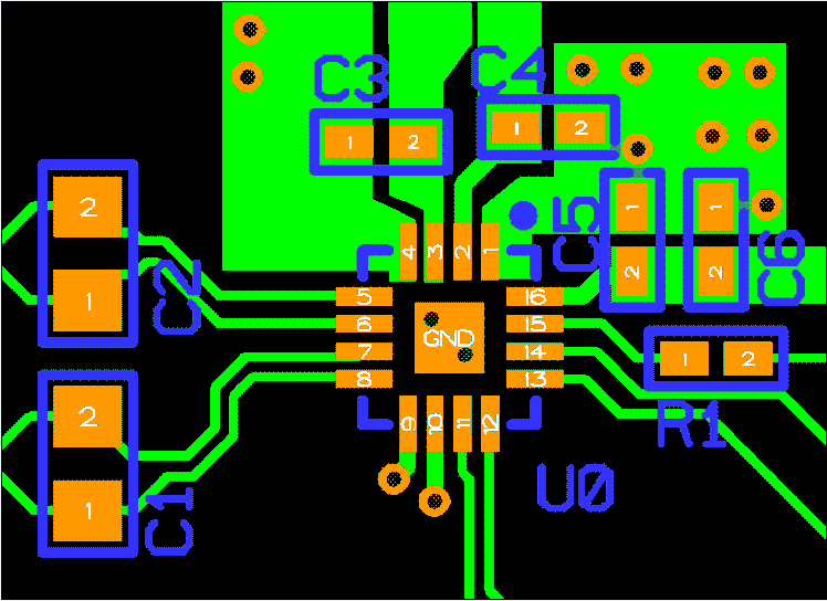
A common ground plane for both analog and digital often gives better results. Typically, the second PCB layer is the ground plane. The ADC ground pins are returned to the ground plane through multiple vias (PTH). Good practice is to place analog components on one side and digital components on other side of the ADC (or ADCs). All signals must be routed, assuming there is a split ground plane for analog and digital. Furthermore, splitting the ground initially during layout is better. Route all analog and digital traces so that the traces see the respective ground all along the second layer. Then short both grounds to form a common ground plane. Figure 56 shows a typical layout around the ADC.
 Figure 56. Recommended ADC Layout
(Only top layer is shown, second layer is common ground for analog and digital)