SLAS708A September 2010 – September 2019 ADS7947 , ADS7948 , ADS7949
PRODUCTION DATA.
- 1 Features
- 2 Applications
- 3 Description
- 4 Revision History
- 5 Device Comparison Table
- 6 Pin Configuration and Functions
-
7 Specifications
- 7.1 Absolute Maximum Ratings
- 7.2 ESD Ratings
- 7.3 Recommended Operating Conditions: ADS794x (12-, 10-, 8-Bit)
- 7.4 Thermal Information
- 7.5 Electrical Characteristics: ADS7947 (12-Bit)
- 7.6 Electrical Characteristics: ADS7948 (10-Bit)
- 7.7 Electrical Characteristics: ADS7949 (8-Bit)
- 7.8 Timing Requirements
- 7.9 Switching Characteristics
- 7.10 Typical Characteristics: ADS7947, ADS7948, ADS7949
- 7.11 Typical Characteristics: ADS7947 (12-Bit)
- 8 Detailed Description
- 9 Application and Implementation
- 10Power Supply Recommendations
- 11Layout
- 12Device and Documentation Support
- 13Mechanical, Packaging, and Orderable Information
Package Options
Mechanical Data (Package|Pins)
- RTE|16
Thermal pad, mechanical data (Package|Pins)
- RTE|16
Orderable Information
8.3.2 Reference
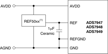
The ADS7947, ADS7948, and ADS7949 use an external reference voltage during the conversion of a sampled signal. The devices switch the capacitors used in the conversion process to the reference terminal during conversion. The switching frequency is the same as the SCLK frequency. The REF terminal must be decoupled to REFGND with a 1-µF ceramic capacitor in order to get the best noise performance from the device. The capacitor must be placed closest to these pins. The reference input can be driven with the REF50xx series precision references from TI. Figure 42 shows a typical reference driving circuit.
For convenience, AVDD can be used as a reference. The ADS794x allow reference ranges up to AVDD. However, make sure that AVDD is well-bypassed and that there is a separate bypass capacitor between REF and REFGND.

NOINDENT:
Select the appropriate device as described by the required reference value. For example, select the REF5040 for a 4-V reference, the REF5030 for a 3-V reference, and the REF5025 for a 2.5-V reference. Ensure that (AVDD – REF) > 0.2 V so that the REF50xx functions properly.