SLASF77A December 2022 – September 2023 AFE11612-SEP
PRODUCTION DATA
- 1
- 1 Features
- 2 Applications
- 3 Description
- 4 Revision History
- 5 Pin Configuration and Functions
-
6 Specifications
- 6.1 Absolute Maximum Ratings
- 6.2 ESD Ratings
- 6.3 Recommended Operating Conditions
- 6.4 Thermal Information
- 6.5 Electrical Characteristics
- 6.6 Timing Characteristics
- 6.7 Timing Diagrams
- 6.8 Typical Characteristics: DAC
- 6.9 Typical Characteristics: ADC
- 6.10 Typical Characteristics: Internal Reference
- 6.11 Typical Characteristics: Temperature Sensor
- 6.12 Typical Characteristics: Digital Inputs
-
7 Detailed Description
- 7.1 Overview
- 7.2 Functional Block Diagram
- 7.3
Feature Description
- 7.3.1
Primary ADC Operation
- 7.3.1.1 Analog Inputs
- 7.3.1.2 ADC Trigger Signals (See AFE configuration register 0 )
- 7.3.1.3 Double-Buffered ADC Data Registers
- 7.3.1.4 SCLK Clock Noise Reduction
- 7.3.1.5 Data Available Pin (DAV)
- 7.3.1.6 Convert Pin (CNVT)
- 7.3.1.7 Analog Input Out-of-Range Detection (See The Analog Input Out-of-Range Alarm Section)
- 7.3.1.8 Full-Scale Range of the Analog Input
- 7.3.2 Secondary ADC and Temperature Sensor Operation
- 7.3.3 Reference Operation
- 7.3.4 DAC Operation
- 7.3.5 Alarm Operation
- 7.3.6 General-Purpose Input and Output Pins (GPIO-0 To GPIO-7)
- 7.3.7 Device Reset Options
- 7.3.1
Primary ADC Operation
- 7.4 Device Functional Modes
- 7.5 Programming
- 7.6
Register Maps
- 7.6.1 Temperature Data Registers (Read-Only)
- 7.6.2 Temperature Configuration (TEMP_CONFIG) Register (address = 0Ah) [reset = 003Ch or 3CFFh]
- 7.6.3 Temperature Conversion Rate (TEMP_CONV_RATE) Register (address = 0Bh) [reset = 0007h or 07FFh]
- 7.6.4 η-Factor Correction Registers: D1_N_ADJUST and D2_N_ADJUST (address = 21h and 22h) [reset = 0000h or 00FFh]
- 7.6.5 ADC-n-Data (ADC_n) Registers (addresses = 23h to 32h) [reset = 0000h]
- 7.6.6 DAC-n-Data (DAC_n) Registers (addresses = 33h to 3Eh) [reset = 0000h)
- 7.6.7 DAC-n-CLR-Setting (DAC_n_CLR) Registers (addresses = 3Fh to 4Ah) [reset = 0000h]
- 7.6.8 GPIO Register (address = 4Bh) [reset = 00FFh]
- 7.6.9 AFE Configuration Register 0 (AFE_CONFIG_0) (address = 4Ch) [reset = 2000h]
- 7.6.10 AFE Configuration Register 1 (AFE_CONFIG_1) (Address = 4Dh) [reset = 0070h]
- 7.6.11 Alarm Control Register (ALR_CTRL) (address = 4Eh) [reset = 0000h]
- 7.6.12 STATUS Register (Address = 4Fh) [reset = 0000h]
- 7.6.13 ADC Channel Register 0 (ADC_CH0) (address = 50h) [reset = 0000h]
- 7.6.14 ADC Channel Register 1 (ADC_CH1) (address = 51h) [reset = 0000h]
- 7.6.15 ADC Gain Register (ADC_GAIN) (address = 52h) [reset = FFFFh]
- 7.6.16 AUTO_DAC_CLR_SOURCE Register (address = 53h) [reset = 0004h]
- 7.6.17 AUTO_DAC_CLR_EN Register (address = 54h) [reset = 0000h]
- 7.6.18 SW_DAC_CLR Register (address = 55h) [reset = 0000h]
- 7.6.19 HW_DAC_CLR_EN_0 Register (address = 56h) [reset = 0000h]
- 7.6.20 HW_DAC_CLR_EN_1 Register (address = 57h) [reset = 0000h]
- 7.6.21 DAC Configuration (DAC_CONFIG) Register (address = 58h) [reset = 0000h]
- 7.6.22 DAC Gain (DAC_GAIN) Register (address = 59h) [reset = 0000h]
- 7.6.23 Analog Input Channel Threshold Registers (addresses = 5Ah To 61h)
- 7.6.24
Temperature Threshold Registers
- 7.6.24.1 LT_HIGH_THRESHOLD Register (address = 62h) [reset = 07FFh, +255.875°C]
- 7.6.24.2 LT_LOW_THRESHOLD Register (address = 63h) [reset = 0800h, –256°C]
- 7.6.24.3 D1_HIGH_THRESHOLD Register (address = 64h) [reset = 07FFh, +255.875°C]
- 7.6.24.4 D1_LOW_THRESHOLD Register (address = 65h) [reset = 0800h, –256°C]
- 7.6.24.5 D2_HIGH_THRESHOLD Register (address = 66h) [reset = 07FFh, +255.875°C]
- 7.6.24.6 D2_LOW_THRESHOLD Register (address = 67h) [reset = 0800h, –256°C]
- 7.6.25 Hysteresis Registers
- 7.6.26 Power-Down Register (PWR_DOWN) (address = 6Bh) [reset = 0000h)
- 7.6.27 Device ID Register (DEVICE_ID) (read only address = 6Ch) [reset = 1220h]
- 7.6.28 Software Reset (SW_RST) Register (read or write address = 7Ch) [reset = N/A)
- 8 Application and Implementation
- 9 Device and Documentation Support
- 10Mechanical, Packaging, and Orderable Information
Package Options
Mechanical Data (Package|Pins)
- PAP|64
Thermal pad, mechanical data (Package|Pins)
- PAP|64
Orderable Information
7.3.2 Secondary ADC and Temperature Sensor Operation
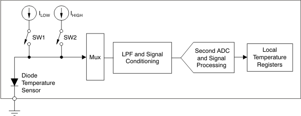
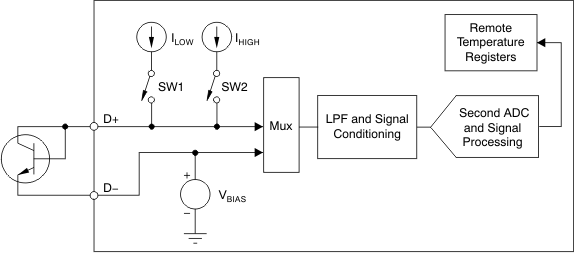
The device contains one local and two remote temperature sensors. The temperature sensors continuously monitor the three temperature inputs, and new readings are automatically available every cycle. The on-chip integrated temperature sensor (shown in Figure 7-4) is used to measure the device temperature. Two remote diode sensor inputs are used to measure the two external temperatures. All analog signals are converted by the secondary ADC that runs in the background at a lower speed. The measurement relies on the characteristics of a semiconductor junction operation at a fixed current level. The forward voltage of the diode (VBE) depends on the current passing through the diode and the ambient temperature. The change in VBE when the diode operates at two different currents (a low current of ILOW and a high current of IHIGH) is shown in Equation 1:

where:
- k is Boltzmann's constant.
- q is the charge of the carrier.
- T is the absolute temperature in kelvins (K).
- η is the ideality of the transistor as a sensor.
 Figure 7-4 Integrated Local Temperature Sensor
The remote sensing transistor can be a discrete, small-signal type transistor or a substrate transistor built within the microprocessor. This architecture is shown in Figure 7-5. An internal voltage source biases the D– pin above ground to prevent the ground noise from interfering with measurement. An external capacitor (up to 330 pF) can be placed between D+ and D– to further reduce noise interference.
 Figure 7-5 Remote Temperature Sensor
The device has three temperature sensors: two remote (D1 and D2) and one on-chip (LT). If any sensor is not used, the sensor can be disabled by clearing the corresponding enable bit (bits D2EN, D1EN, and LTEN of the temperature configuration register). When disabled, the sensors are not converted. The device continuously monitors the selected temperature sensors in the background, leaving the user free to perform conversions on the other channels. When one monitor cycle finishes, a signal passes to the control logic to automatically initiate a new conversion.
The analog sensing signal is preprocessed by a low-pass filter and signal-conditioning circuitry, and then digitized by the ADC. The resulting digital signal is further processed by the digital filter and processing unit. The final result is stored in the LT-temperature-data register, the D1-temperature-data register, and the D2-temperature-data register, respectively. The format of the final result is in 2's complement, as shown in Table 7-1.
| TEMPERATURE (°C) | DIGITAL CODE |
|---|---|
| +255.875 | 011111111111 |
| +150 | 010010110000 |
| +100 | 001100100000 |
| +50 | 000110010000 |
| +25 | 000011001000 |
| +1 | 000000001000 |
| 0 | 000000000000 |
| –1 | 111111111000 |
| –25 | 111100111000 |
| –50 | 111001110000 |
| –100 | 110011100000 |
| –150 | 101101010000 |
| –256 | 100000000000 |