SLASF77A December 2022 – September 2023 AFE11612-SEP
PRODUCTION DATA
- 1
- 1 Features
- 2 Applications
- 3 Description
- 4 Revision History
- 5 Pin Configuration and Functions
-
6 Specifications
- 6.1 Absolute Maximum Ratings
- 6.2 ESD Ratings
- 6.3 Recommended Operating Conditions
- 6.4 Thermal Information
- 6.5 Electrical Characteristics
- 6.6 Timing Characteristics
- 6.7 Timing Diagrams
- 6.8 Typical Characteristics: DAC
- 6.9 Typical Characteristics: ADC
- 6.10 Typical Characteristics: Internal Reference
- 6.11 Typical Characteristics: Temperature Sensor
- 6.12 Typical Characteristics: Digital Inputs
-
7 Detailed Description
- 7.1 Overview
- 7.2 Functional Block Diagram
- 7.3
Feature Description
- 7.3.1
Primary ADC Operation
- 7.3.1.1 Analog Inputs
- 7.3.1.2 ADC Trigger Signals (See AFE configuration register 0 )
- 7.3.1.3 Double-Buffered ADC Data Registers
- 7.3.1.4 SCLK Clock Noise Reduction
- 7.3.1.5 Data Available Pin (DAV)
- 7.3.1.6 Convert Pin (CNVT)
- 7.3.1.7 Analog Input Out-of-Range Detection (See The Analog Input Out-of-Range Alarm Section)
- 7.3.1.8 Full-Scale Range of the Analog Input
- 7.3.2 Secondary ADC and Temperature Sensor Operation
- 7.3.3 Reference Operation
- 7.3.4 DAC Operation
- 7.3.5 Alarm Operation
- 7.3.6 General-Purpose Input and Output Pins (GPIO-0 To GPIO-7)
- 7.3.7 Device Reset Options
- 7.3.1
Primary ADC Operation
- 7.4 Device Functional Modes
- 7.5 Programming
- 7.6
Register Maps
- 7.6.1 Temperature Data Registers (Read-Only)
- 7.6.2 Temperature Configuration (TEMP_CONFIG) Register (address = 0Ah) [reset = 003Ch or 3CFFh]
- 7.6.3 Temperature Conversion Rate (TEMP_CONV_RATE) Register (address = 0Bh) [reset = 0007h or 07FFh]
- 7.6.4 η-Factor Correction Registers: D1_N_ADJUST and D2_N_ADJUST (address = 21h and 22h) [reset = 0000h or 00FFh]
- 7.6.5 ADC-n-Data (ADC_n) Registers (addresses = 23h to 32h) [reset = 0000h]
- 7.6.6 DAC-n-Data (DAC_n) Registers (addresses = 33h to 3Eh) [reset = 0000h)
- 7.6.7 DAC-n-CLR-Setting (DAC_n_CLR) Registers (addresses = 3Fh to 4Ah) [reset = 0000h]
- 7.6.8 GPIO Register (address = 4Bh) [reset = 00FFh]
- 7.6.9 AFE Configuration Register 0 (AFE_CONFIG_0) (address = 4Ch) [reset = 2000h]
- 7.6.10 AFE Configuration Register 1 (AFE_CONFIG_1) (Address = 4Dh) [reset = 0070h]
- 7.6.11 Alarm Control Register (ALR_CTRL) (address = 4Eh) [reset = 0000h]
- 7.6.12 STATUS Register (Address = 4Fh) [reset = 0000h]
- 7.6.13 ADC Channel Register 0 (ADC_CH0) (address = 50h) [reset = 0000h]
- 7.6.14 ADC Channel Register 1 (ADC_CH1) (address = 51h) [reset = 0000h]
- 7.6.15 ADC Gain Register (ADC_GAIN) (address = 52h) [reset = FFFFh]
- 7.6.16 AUTO_DAC_CLR_SOURCE Register (address = 53h) [reset = 0004h]
- 7.6.17 AUTO_DAC_CLR_EN Register (address = 54h) [reset = 0000h]
- 7.6.18 SW_DAC_CLR Register (address = 55h) [reset = 0000h]
- 7.6.19 HW_DAC_CLR_EN_0 Register (address = 56h) [reset = 0000h]
- 7.6.20 HW_DAC_CLR_EN_1 Register (address = 57h) [reset = 0000h]
- 7.6.21 DAC Configuration (DAC_CONFIG) Register (address = 58h) [reset = 0000h]
- 7.6.22 DAC Gain (DAC_GAIN) Register (address = 59h) [reset = 0000h]
- 7.6.23 Analog Input Channel Threshold Registers (addresses = 5Ah To 61h)
- 7.6.24
Temperature Threshold Registers
- 7.6.24.1 LT_HIGH_THRESHOLD Register (address = 62h) [reset = 07FFh, +255.875°C]
- 7.6.24.2 LT_LOW_THRESHOLD Register (address = 63h) [reset = 0800h, –256°C]
- 7.6.24.3 D1_HIGH_THRESHOLD Register (address = 64h) [reset = 07FFh, +255.875°C]
- 7.6.24.4 D1_LOW_THRESHOLD Register (address = 65h) [reset = 0800h, –256°C]
- 7.6.24.5 D2_HIGH_THRESHOLD Register (address = 66h) [reset = 07FFh, +255.875°C]
- 7.6.24.6 D2_LOW_THRESHOLD Register (address = 67h) [reset = 0800h, –256°C]
- 7.6.25 Hysteresis Registers
- 7.6.26 Power-Down Register (PWR_DOWN) (address = 6Bh) [reset = 0000h)
- 7.6.27 Device ID Register (DEVICE_ID) (read only address = 6Ch) [reset = 1220h]
- 7.6.28 Software Reset (SW_RST) Register (read or write address = 7Ch) [reset = N/A)
- 8 Application and Implementation
- 9 Device and Documentation Support
- 10Mechanical, Packaging, and Orderable Information
Package Options
Mechanical Data (Package|Pins)
- PAP|64
Thermal pad, mechanical data (Package|Pins)
- PAP|64
Orderable Information
7.3.2.2 Ideality Factor
The ideality factor (η) is a measured characteristic of a remote temperature sensor diode as compared to an ideal diode. The device allows for different η-factor values, according to Table 7-2. The device is trimmed for a power-on reset (POR) value of η = 1.008. If η is different, the η-factor correction register can be used. The value (NADJUST) written in this register must be in 2's complement format, as shown in Table 7-2. This value is used to adjust the effective η-factor according to Equation 2 and Equation 3.
Table 7-2 η-Factor Range (Single Byte)
| NADJUST | ηEFF | ||
|---|---|---|---|
| BINARY | HEX | DECIMAL | |
| 0111 1111 | 7F | 127 | 1.747977 |
| 0000 1010 | 0A | 10 | 1.042759 |
| 0000 1000 | 08 | 8 | 1.035616 |
| 0000 0110 | 06 | 6 | 1.028571 |
| 0000 0100 | 04 | 4 | 1.021622 |
| 0000 0010 | 02 | 2 | 1.014765 |
| 0000 0001 | 01 | 1 | 1.011371 |
| 0000 0000 | 00 | 0 | 1.008 |
| 1111 1111 | FF | –1 | 1.004651 |
| 1111 1110 | FE | –2 | 1.001325 |
| 1111 1100 | FC | –4 | 0.994737 |
| 1111 1010 | FA | –6 | 0.988235 |
| 1111 1000 | F8 | –8 | 0.981818 |
| 1111 0110 | F6 | –10 | 0.975484 |
| 1000 0000 | 80 | –128 | 0.706542 |
Equation 2. 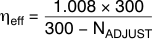
Equation 3. 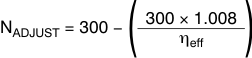
where:
- ηEFF is the actual ideality of the transistor used and
- NADJUST is the corrected ideality used in the calculation.