SLUSE97 November 2023 BQ76905
PRODUCTION DATA
- 1
- 1 Features
- 2 Applications
- 3 Description
- 4 Device Comparison Table
- 5 Pin Configuration and Functions
-
6 Specifications
- 6.1 Absolute Maximum Ratings
- 6.2 ESD Ratings
- 6.3 Recommended Operating Conditions
- 6.4 Thermal Information
- 6.5 Supply Current
- 6.6 Digital I/O
- 6.7 REGOUT LDO
- 6.8 Voltage References
- 6.9 Coulomb Counter
- 6.10 Coulomb Counter Digital Filter
- 6.11 Current Wake Detector
- 6.12 Analog-to-Digital Converter
- 6.13 Cell Balancing
- 6.14 Internal Temperature Sensor
- 6.15 Thermistor Measurement
- 6.16 Hardware Overtemperature Detector
- 6.17 Internal Oscillator
- 6.18 Charge and Discharge FET Drivers
- 6.19 Comparator-Based Protection Subsystem
- 6.20 Timing Requirements—I2C Interface, 100-kHz Mode
- 6.21 Timing Requirements—I2C Interface, 400-kHz Mode
- 6.22 Timing Diagram
- 6.23 Typical Characteristics
- 7 Detailed Description
- 8 Application and Implementation
- 9 Device and Documentation Support
- 10Revision History
- 11Mechanical, Packaging, and Orderable Information
Package Options
Mechanical Data (Package|Pins)
- RGR|20
Thermal pad, mechanical data (Package|Pins)
- RGR|20
Orderable Information
8.2.6 FET Driver Turn-Off
The low-side CHG and DSG FET drivers operate differently when they are triggered to turn off their respective FET. The DSG driver includes an internal switch that drives the DSG pin toward the VSS pin level when the driver is disabled. The driver is specified with a maximum fall time into a 20-nF capacitive load, with 100-Ω series resistance between the DSG pin and the DSG gate. If the driver is used with a larger capacitive load, the fall time generally increases. The system designer can optimize the series resistance value based on the board components and DSG FET(s) used.
The external series gate resistor between the DSG pin and the DSG FET gate is used to adjust the speed of the turn-off transient. A low resistance (such as 100 Ω) provides a fast turn-off during a short circuit event, but this can result in an overly large inductive spike at the top of stack when the FET is disabled. A larger resistor value (such as 1 kΩ or 4.7 kΩ) reduces this speed and the corresponding inductive spike level.
The CHG FET driver discharges the CHG pin toward the VSS pin level, but it includes an additional series PFET in order to support voltages below VSS. This is generally needed when a pack is heavily discharged, for example, if cells in a 5S pack are at 2.5 V per cell, then PACK+ = 12.5 V relative to device VSS. Then if a charger is attached while the CHG FET is disabled and applies a full charge voltage across PACK+ relative to PACK-, such as 4.3 V per cell, or 21.5 V for the 5S pack, this results in PACK– dropping to approximately –9 V relative to VSS. In order to keep the CHG FET disabled, its gate voltage must drop to near this –9 V level.
To support this type of case, the CHG FET driver in BQ76905 is designed to withstand voltages as low as –25 V (recommended) relative to the VSS pin voltage by including a series PFET at the pin, with its gate connected to VSS. When the CHG driver is disabled, the driver pulls the pin voltage downward. As the pin voltage nears VSS, the PFET is disabled, so the pin becomes high impedance. At this point, the external gate-source resistor on the CHG FET pulls the pin voltage lower to the PACK– level, keeping the CHG FET disabled.
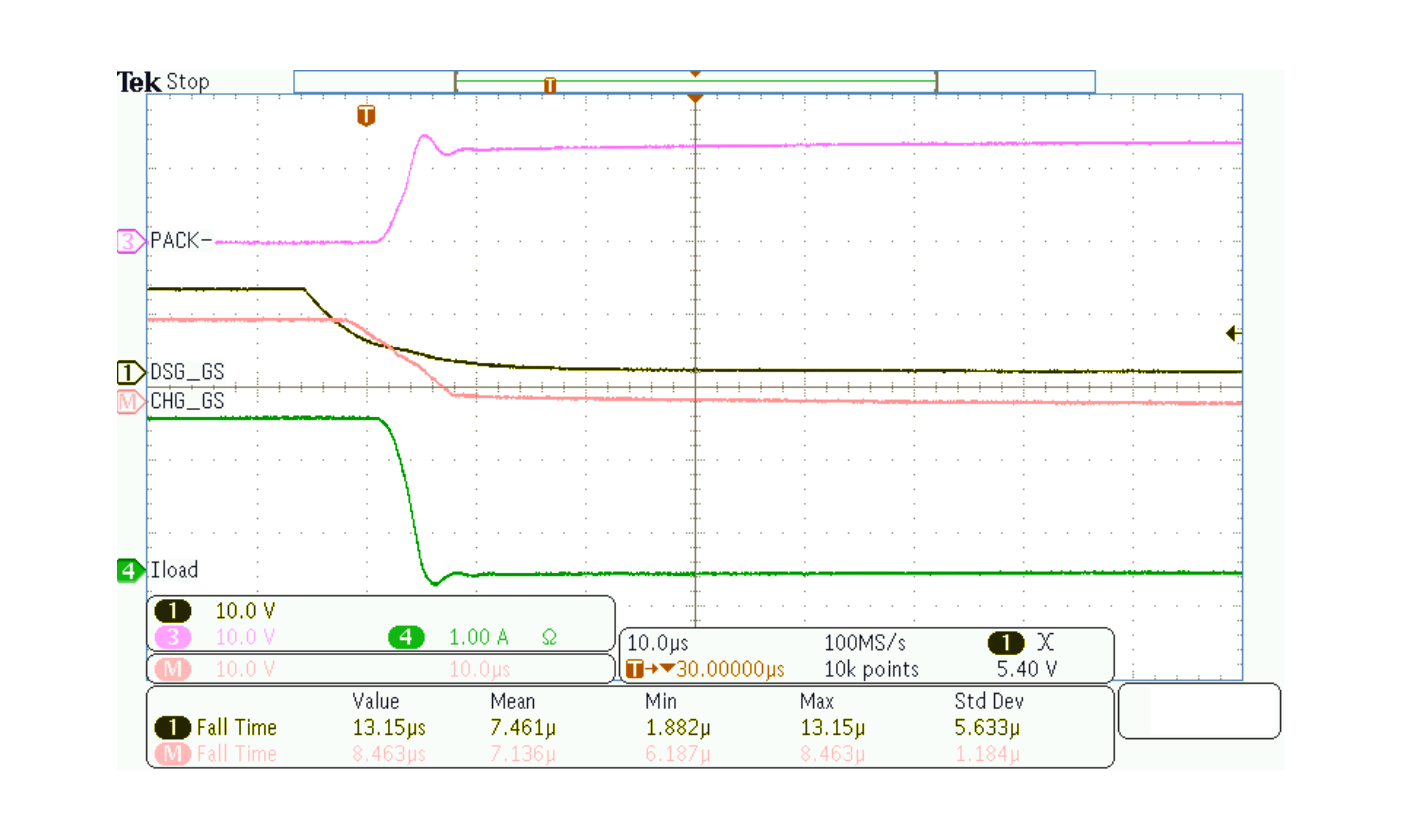
Oscilloscope captures of CHG and DSG driver turn-off are shown below, with the pins driving the gates of CSD18532Q5B NFETs, which have a typical Ciss of 3900 pF. Figure 8-12 shows the signals when using a 1.35-kΩ series gate resistor between the DSG pin and the FET gate, and a 2A load connected between PACK+ and PACK–.
 Figure 8-6 Moderate Speed DSG FET
Turn-Off, Using a 1.35-kΩ Series Gate Resistor, and a 2A Load between PACK+ and
PACK–.
Figure 8-6 Moderate Speed DSG FET
Turn-Off, Using a 1.35-kΩ Series Gate Resistor, and a 2A Load between PACK+ and
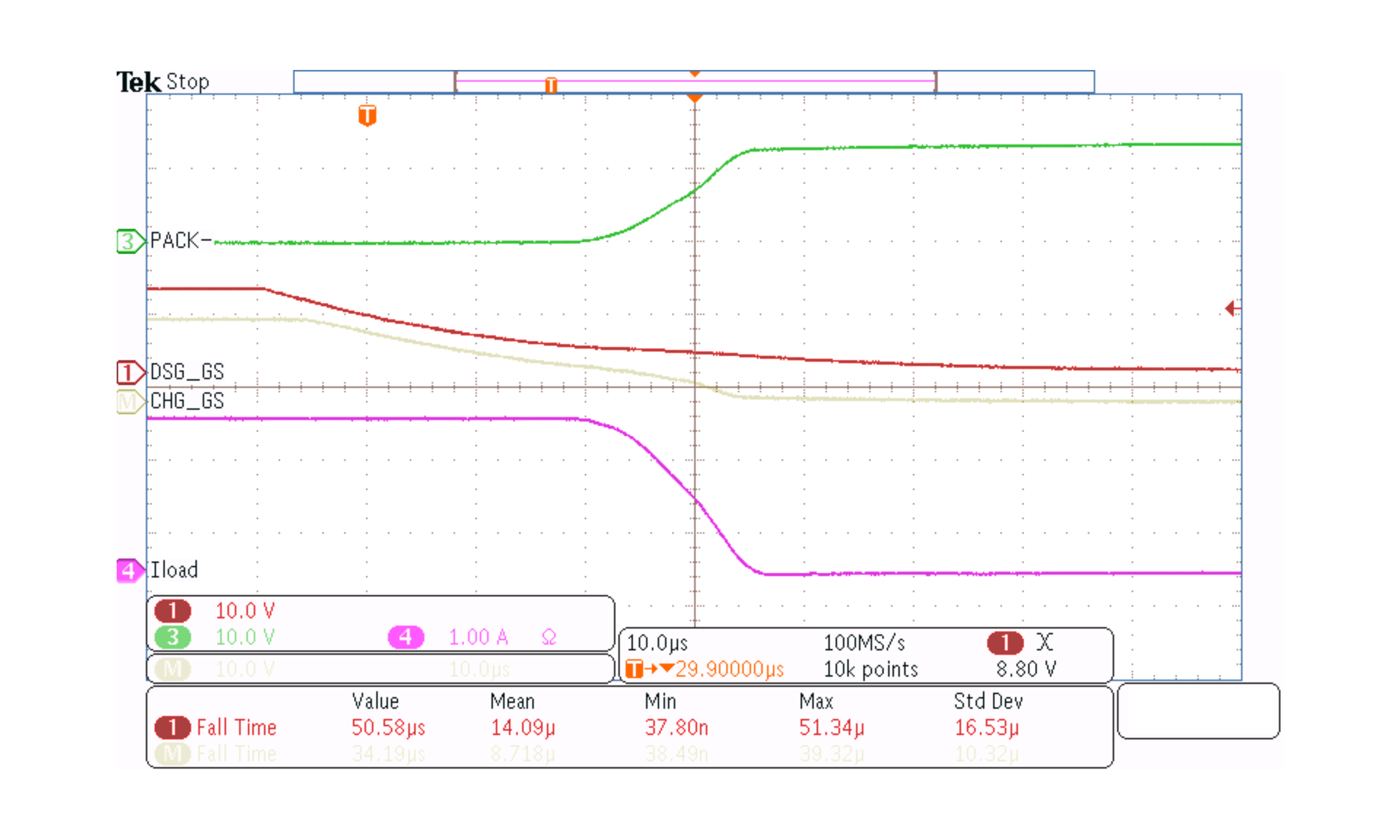
PACK–.A slower turn-off case is shown in Figure 8-7, using a 4.5-kΩ series gate resistor, and a 2A load between PACK+ and PACK–.
 Figure 8-7 A Slower Turn-Off Case Using a
4.5-kΩ Series Gate Resistor
Figure 8-7 A Slower Turn-Off Case Using a
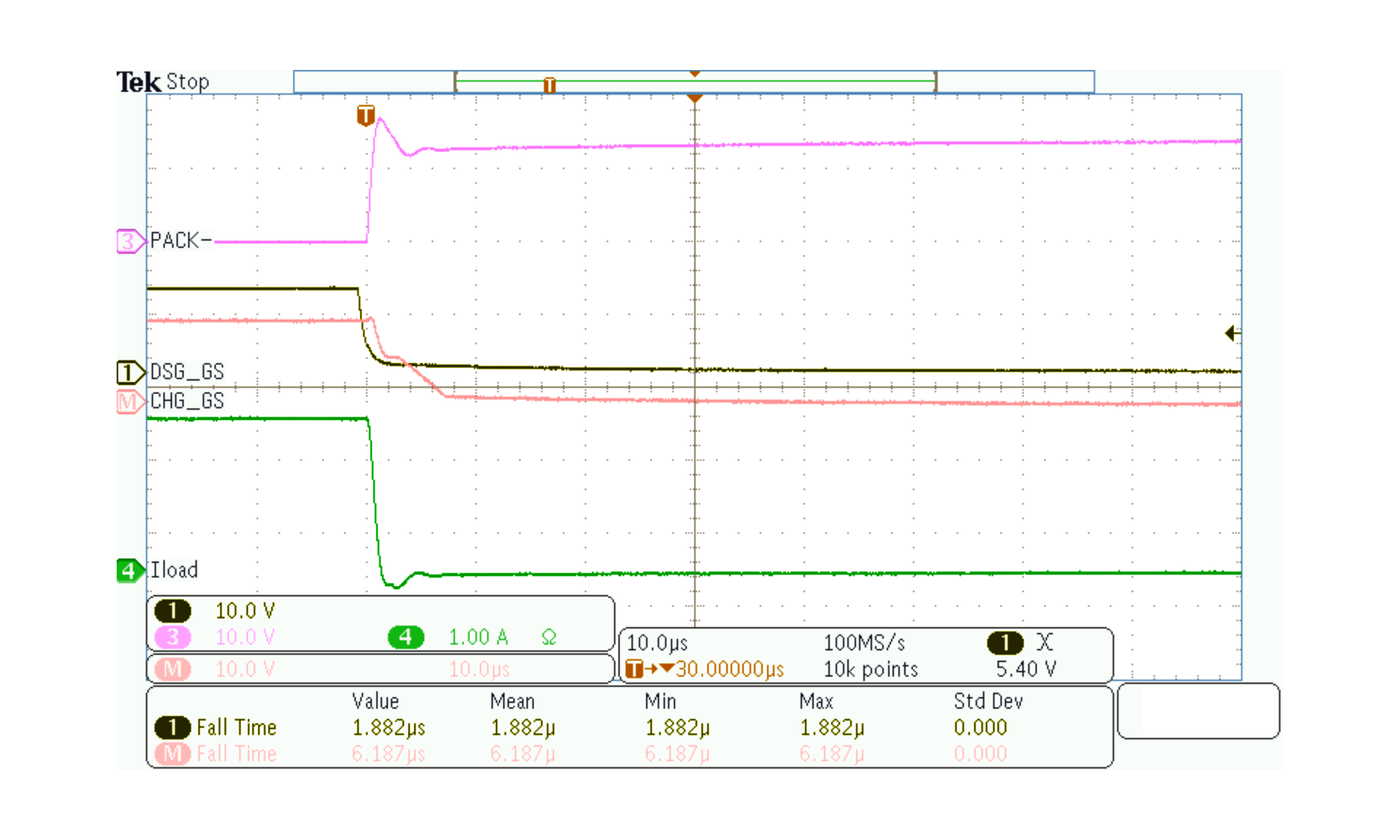
4.5-kΩ Series Gate ResistorA fast turn-off case is shown in Figure 8-8, in which a 100-Ω series gate resistor is used between the DSG pin and the FET gate.
 Figure 8-8 A Fast Turn-Off Case with a
100-Ω Series Gate Resistor