SLUSE97 November 2023 BQ76905
PRODUCTION DATA
- 1
- 1 Features
- 2 Applications
- 3 Description
- 4 Device Comparison Table
- 5 Pin Configuration and Functions
-
6 Specifications
- 6.1 Absolute Maximum Ratings
- 6.2 ESD Ratings
- 6.3 Recommended Operating Conditions
- 6.4 Thermal Information
- 6.5 Supply Current
- 6.6 Digital I/O
- 6.7 REGOUT LDO
- 6.8 Voltage References
- 6.9 Coulomb Counter
- 6.10 Coulomb Counter Digital Filter
- 6.11 Current Wake Detector
- 6.12 Analog-to-Digital Converter
- 6.13 Cell Balancing
- 6.14 Internal Temperature Sensor
- 6.15 Thermistor Measurement
- 6.16 Hardware Overtemperature Detector
- 6.17 Internal Oscillator
- 6.18 Charge and Discharge FET Drivers
- 6.19 Comparator-Based Protection Subsystem
- 6.20 Timing Requirements—I2C Interface, 100-kHz Mode
- 6.21 Timing Requirements—I2C Interface, 400-kHz Mode
- 6.22 Timing Diagram
- 6.23 Typical Characteristics
- 7 Detailed Description
- 8 Application and Implementation
- 9 Device and Documentation Support
- 10Revision History
- 11Mechanical, Packaging, and Orderable Information
Package Options
Mechanical Data (Package|Pins)
- RGR|20
Thermal pad, mechanical data (Package|Pins)
- RGR|20
Orderable Information
8.2.5 Startup Timing
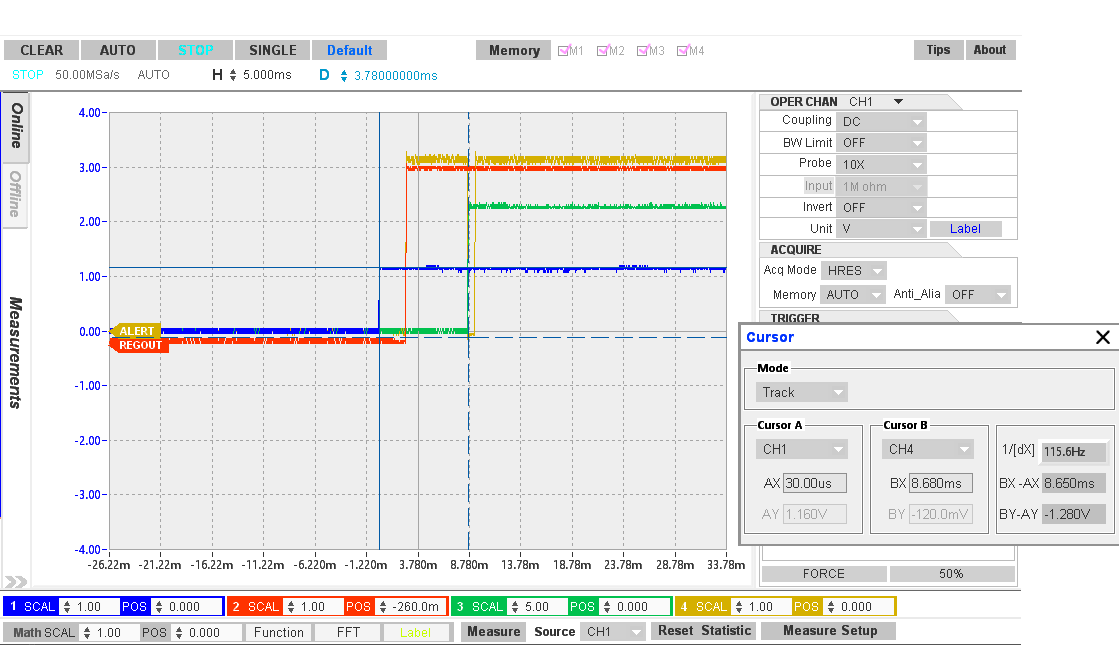
At initial power-up of the BQ76905 device from a SHUTDOWN state, the device progresses through a sequence of events before entering NORMAL mode operation. These are described in Table 8-2 for an example configuration, with approximate timing shown.
| STEP | COMMENT | APPROXIMATE TIME (RELATIVE TO WAKEUP EVENT) |
|---|---|---|
| Wakeup event | Either the TS pin or the VC0 pin is pulled up, triggering the device to exit SHUTDOWN mode | 0 |
| REGOUT powered | Measured with the OTP programmed to autonomously power the REGOUT LDO | 2.6 ms |
| First Cell-1 measurement completed | Data from first measurement of Cell-1 can be read back | 3.2 ms |
| INITCOMP, ADSCAN, and FULLSCAN asserted (5 series) | Measured with the OTP programmed to provide the INITCOMP and ADSCAN bits in the Alarm signal on the ALERT pin [CVADCSPEED1:0] = 0x0, [IADCSPEED1:0] = 0x0, [SSADCSPEED1:0] = 0x0 | 8.6 ms |
| FETs enabled (5 series) | Measured with the OTP programmed to autonomously enable FETs. [CVADCSPEED1:0] = 0x0, [IADCSPEED1:0] = 0x0, [SSADCSPEED1:0] = 0x0 | 8.6 ms |
Figure 8-5 shows an example of an oscilloscope plot of a startup sequence with the device configured in OTP for a 5-series pack, with [FET_EN] = 1 for autonomous FET control and providing the [INITCOMP] flag on the ALERT pin. The TS pin is pulled up to initiate device wakeup from SHUTDOWN. The TS pin voltage is shown in blue; the DSG pin voltage is shown in green.
 Figure 8-5 Startup Sequence for a
5-Series Pack