SBOS571C August   2011  – August 2018 BUF20800-Q1

PRODUCTION DATA.  

  1. Features
  2. Applications
  3. Description
    1.     Device Images
      1.      Simplified Block Diagram
  4. Revision History
  5. Pin Configuration and Functions
    1.     Pin Functions
  6. Specifications
    1. 6.1 Absolute Maximum Ratings
    2. 6.2 ESD Ratings
    3. 6.3 Recommended Operating Conditions
    4. 6.4 Thermal Information
    5. 6.5 Electrical Characteristics
    6. 6.6 Typical Characteristics
  7. Detailed Description
    1. 7.1 Overview
    2. 7.2 Functional Block Diagram
    3. 7.3 Feature Description
      1. 7.3.1 General-call Reset and Power-up
      2. 7.3.2 Output Voltage
      3. 7.3.3 Output Latch
      4. 7.3.4 Programmable VCOM
      5. 7.3.5 REFH and REFL Input range
    4. 7.4 Device Functional Modes
      1. 7.4.1 Replacement of Traditional Gamma Buffer
      2. 7.4.2 Dynamic Gamma Control
    5. 7.5 Programming
      1. 7.5.1 Two-wire Bus Overview
      2. 7.5.2 Data Rates
      3. 7.5.3 Read/Write Operations
        1. 7.5.3.1 Writing
        2. 7.5.3.2 Reading
      4. 7.5.4 Register Maps
        1. 7.5.4.1 Addressing the BUF20800-Q1
      5. 7.5.5 Registers
  8. Application and Implementation
    1. 8.1 Application Information
    2. 8.2 Typical Application
      1. 8.2.1 Design Requirements
      2. 8.2.2 Detailed Design Procedure
        1. 8.2.2.1 Input Capacitor Selection
        2. 8.2.2.2 REFH and REFL Voltage Settings
      3. 8.2.3 Application Curves
      4. 8.2.4 Configuration for 20 Gamma Channels
      5. 8.2.5 Configuration for 22 Gamma Channels
      6. 8.2.6 The BUF20800-Q1 in Industrial Applications
      7. 8.2.7 Total TI Panel Solution
  9. Power Supply Recommendations
  10. 10Layout
    1. 10.1 Layout Guidelines
      1. 10.1.1 General PowerPAD Design Considerations
    2. 10.2 Layout Example
  11. 11Device and Documentation Support
    1. 11.1 Documentation Support
      1. 11.1.1 Related Documentation
    2. 11.2 Receiving Notification of Documentation Updates
    3. 11.3 Community Resources
    4. 11.4 Trademarks
    5. 11.5 Electrostatic Discharge Caution
    6. 11.6 Glossary
  12. 12Mechanical, Packaging, and Orderable Information

Package Options

Mechanical Data (Package|Pins)
Thermal pad, mechanical data (Package|Pins)
Orderable Information

Programmable VCOM

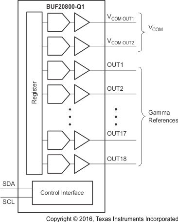
The VCOM channels of the BUF20800-Q1 can swing to 2V from the positive supply rail while sourcing 50 mA and to 1 V above the negative rail while sinking 50 mA (see Figure 4, typical characteristic Output Voltage vs Output Current). To store the gamma and the VCOM values, an external EEPROM is required. During power-up of the LCD panel, the timing controller can then read the EEPROM and load the values into the BUF20800-Q1 to generate the desired VCOM voltages, as illustrated in Figure 10 and Figure 8. The VCOM channels can be programmed independently from the gamma channels.
BUF20800-Q1 appinfo_buffprogvcom_SBOS571.gifFigure 8. BUF20800-Q1 Used for Programmable VCOM